Continue to Site

Welcome to EDAboard.com

Welcome to our site! EDAboard.com is an international Electronics Discussion Forum focused on EDA software, circuits, schematics, books, theory, papers, asic, pld, 8051, DSP, Network, RF, Analog Design, PCB, Service Manuals... and a whole lot more! To participate you need to register. Registration is free. Click here to register now.

Modified Square Wave Inverter

Status
Not open for further replies.

engr.waqas

Full Member level 3
Joined
Jul 21, 2009
Messages
172
Helped
13
Reputation
26
Reaction score
10
Trophy points
1,298
Location
karachi,Pakistan
Activity points
2,342
Hi
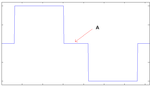
As you know the modified square wave inverter has wave form which comes to zero for some time before going high or low as shown in attached diagram . I want to ask you that why we can't achieve this point "A" in diagram by simply turning off transistors for some time (using microcontroller) and then turn on them to get high and low pulses. Why we need PWM to do this task ?
 

Attachments

  • untitled.PNG
    untitled.PNG
    8.5 KB · Views: 69

I want to ask you that why we can't achieve this point "A" in diagram by simply turning off transistors for some time (using microcontroller) and then turn on them to get high and low pulses.
When the one inverting switch is off, there is no path to discharge that node. That is why point "A" is not achievable. In PWM case you let the output node discharge in a brief amount of time. and then on the other switch.
 

Thanks for your reply.
Can you please explain what do you mean by discharging of a node?
Also it would be great help for me if you can refer me a literature on web which explain the working of modified square wave inverter.
 

why we can't achieve this point "A" in diagram by simply turning off transistors for some time (using microcontroller) and then turn on them to get high and low pulses. Why we need PWM to do this task ?
You can: the point of the modified square wave inverter is just to avoid the mode expensive PWM!
If your output stage is an H-bridge with flyback diodes you can open a side while leaving turned on the other one.
For example, suppose that the left side is high and the right side is low: to go to A you set the left side to high impedance and leave the right side to low. You do the opposite for the other transition.
 

Read schemit trigger inverter, there it gives sharp cut off falling/ rising.
 

@dave9000 : thanks for your reply
By setting left side to high impedance you mean simply I turn mosfets of these sides off ?. In other words I turn off all the transistors for some time to reach the point A ?
 

yes, and it is very important that you have the diodes in place: if the load is inductive the left voltage will drop below the low rail.
Try simulating the circuit for a couple of cycles with an inductive load to better understand what's going on, you don't want to blow-up your mosfets because of a wrong line of code ;-)
 
Status
Not open for further replies.

Similar threads

Part and Inventory Search

Welcome to EDABoard.com

Sponsor

Back
Top