Continue to Site

Welcome to EDAboard.com

Welcome to our site! EDAboard.com is an international Electronics Discussion Forum focused on EDA software, circuits, schematics, books, theory, papers, asic, pld, 8051, DSP, Network, RF, Analog Design, PCB, Service Manuals... and a whole lot more! To participate you need to register. Registration is free. Click here to register now.

Low offset Op-amp layout guide?

Status
Not open for further replies.

Sajjadkhan

Full Member level 5
Joined
Sep 25, 2010
Messages
307
Helped
17
Reputation
34
Reaction score
16
Trophy points
1,298
Location
Rawalpindi,Pakistan
Activity points
4,199
I want to design a simple precision DC electronic load as those of Bk precision are expensive and they are actually when you think you can build one.

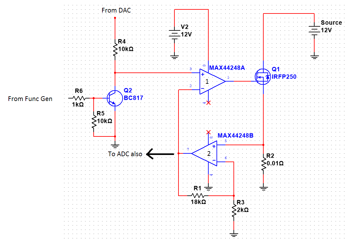
AS you can see in the fig i am using MAX44248 because i have already ordered them.I am not using direct feedback to the op-amp1 but via op-amp2 (gain of 10). Reason is so that i dont have to divide the DAC voltage on +ive input of opamp1.
A transistor at op-amp1 so that i can hook up fun gen to make pulse current.

This load will sink up to 20 Amps and (using multiple fets) and resolution of 1mA.

The opamp has the Vos of 10uV (worst case). so need to know about layout design as i have never designed with such low precision ic.

I know there would be thermocouple effects and ground loop problem, i am currently reading about them. I am designing this on home made PCB (i can design quite neat PCB).

Any suggestions for what i know and i dont know.


Hi,

R2: 20A x 20A X 0.01R = 4W. I recommend to use at least a 10W rated one.
Don´t use a wire wound, because it´s inductivity causes oscillations.

R2 GND connection has to be rock solid. far belwo 0.01R.
R2 needs a current path and different sense path (one to pin5 of OPAMP, the other to R3 instead of GND.

To serialize two opamps and a FET in one regulation loop is critical. expect oscillations. (There is no phase diagram in the datasheet to calculate stability)
Therefore:
* Use some 330pF in parallel to R1 as local HF feedback.
* add a resistor between Pin7 of OPAMP and pin2 of opamp (10k?)
* add a 470pF capacitor from Pin1 to pin2 of opamp

To improve OFF current replace Q2 with a mosfet.
The whole circuit will not be able to react faster than 30kHz. Expect a distorted square wave even with 10kHz.

Place a ceramic capacitor 1uF at least and additionally a low ESR electrolytic capacitor on drain of Q1.
Place a 100nF ceramic capacitor next to pin 8 of OPAMP.

You don´t use negative supply. Therfore you will have a problem regulating down to zero.
I recommend to add a small bias voltage at pin5 of OPAMP. Then you should be able to regulate down to zero, but you have to adjust your DAC to bias voltage (amlified by 10).

Klaus

P.S. do a simulation on that circuit.
 

To serialize two opamps and a FET in one regulation loop is critical. expect oscillations. (There is no phase diagram in the datasheet to calculate stability)
Therefore:
* Use some 330pF in parallel to R1 as local HF feedback.
* add a resistor between Pin7 of OPAMP and pin2 of opamp (10k?)
* add a 470pF capacitor from Pin1 to pin2 of opamp

Thanks. Good Suggestions and you made me understand. But kindly explain these above 3 point in a bit detail.

1. 330pf to make it act like integrator, but will if effect frequency?
2.Affect of 10k?
3.470pf? from pin 1 to Gnd eliminates osc but what will it do from pin1 to pin2?
 

Saj, You ought to specify the constraints of your designs. What is the input and output response desired for rise time, duty cycle, current, vs voltage. There is no mechanical specs either for thermal effects and the loop stability is ignored. These should all come out in your load simulator specs which you can specify in point form.
 

Hi,

1. 330pf to make it act like integrator, but will if effect frequency?
No, not to make it act like an integrator. For low frequency the parallel R is dominant.
But for high frequencies the local gain is limited to 1 cased by the C. f_cutoff = 27kHz
The OPAMP is specified to be unity gain stable, so this should help the whole regulation loop to be stable. But with the 300pF we are on the upper frequency limit, so stability is still influenced by the other OPAMP.
Therefore i recommend to simulate this circuit.

2.Affect of 10k?
3.470pf? from pin 1 to Gnd eliminates osc but what will it do from pin1 to pin2?

The 10k input resistor combined with the 470pF feedback capacitor again forms a local HF feedback with f_cutoff = 34kHz.

BTW: a capacitor from pin1 to GND acts like a short circuit load for HF. But it does not avoid oscillation. Look into the datasheet and find (charts) that the OPAMP is stable when driving no or low value capacitors, but it oscillates (unstable) with higher value capacitors.


Klaus
 

Saj, You ought to specify the constraints of your designs. What is the input and output response .....

Let me help you get started. This should be standard practice for any design.

Inputs
1. from DAC. Analog, low Z 0~2Vdc
- 10K series to Hi Z
- controls Q1 current 10A/Vin
2. From Func Gen, logic 0,7 threshold 1kOhm​

Outputs
- To ADC ( current sense ) 0.1V/A
- Q1 drain to 12V supply, 0~20A

Functions
max rep rate = ? ( 1MHz ?)
Slew rate = ? minimum ( 10A/us? )
Duty Cycle = ? ( 1~99% )
Vgs gain ? gm?
U1 GBW 1MHz Gain = 1e6, BW=1Hz
U2 Gain/BW 10 /
VCM VSS -0.05 to VDD -1.5
Loop gain =?
Unity gain bandwidth = ?
Phase Margin = ?

Environment
Max Tj rise 50'C

Analysis
Q1 gain ~ 10 A/V @ Vgs=4.5
I Sense ~ 0.1V/A
Loop Gain 1e6
 

Status
Not open for further replies.

Part and Inventory Search

Welcome to EDABoard.com

Sponsor

Back
Top