Vermes
Advanced Member level 4

- Joined
- Aug 2, 2011
- Messages
- 1,163
- Helped
- 0
- Reputation
- 0
- Reaction score
- 0
- Trophy points
- 1,316
- Activity points
- 22,318
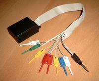
This circuit of analyzer is compatible with SALEAE or USBee software. It allows you to store waveforms of 8 channels with sampling frequency up to 24MHz in the computer. The task is to transfer the samples to the computer via the USB port, further processing is done is the software which allows you to preview the finished frames of several typical protocols without the analysis of slopes and levels.
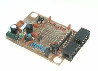
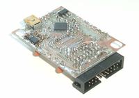
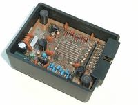
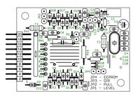
The circuit was inspired by some solutions found on the Internet. There is space for 2 EEPROM on the board, so that you can select (using a jumper) the identifier through which the circuit will be recognized via original software. The jumper on line data also allows you to upload or change the identifier without desoldering EEPROM from the board, through CyConsole from packet Cypress Suite. The entire system consists of typical and easily available components, except the CY7C68013A in housing QFN (it can be purchased via ebay). Schematic also includes placing a level translator 74LVC8T245, but in this case it was omitted while assembling, because in this particular analyzer there was no need to work with levels different than 3,3V or 5V. Inputs were protected with resistors and diodes BAT41. Each input should withstand accidental voltage fed 12V. Inputs can be pulled through resistors 100k to the ground or reference voltage which can be equal 3.3V, 5V, or can be provided from the outside. The main connector has also additional selection signals of direction for the buffer 74LVC8T245 (DIR), external reference voltage which can be also used as auxiliary power output (3,3V or 5V) and signals CLKOUT and TRIG which will be useful for external ADC circuit, for example on AD9280 (32 MSPS).
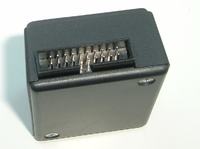
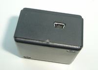
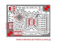
The circuit is adapted for the size of housing Z-68, the PCB was designed as one-sided.
Pictures:
 **broken link removed**
Link to original thread (useful attachment) - Analizator logiczny na CY7C68013A