Continue to Site

Welcome to EDAboard.com

Welcome to our site! EDAboard.com is an international Electronics Discussion Forum focused on EDA software, circuits, schematics, books, theory, papers, asic, pld, 8051, DSP, Network, RF, Analog Design, PCB, Service Manuals... and a whole lot more! To participate you need to register. Registration is free. Click here to register now.

IGBT switching loss control

Status
Not open for further replies.
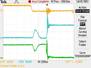
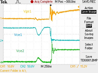
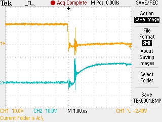
Strictly spoken, the schottky diode's purpose isn't faster turn off rather than keeping the gate voltage safely low when the other switch turns on. The most reliable way to achieve this would be a bipolar gate driver supply. I won't mind the negative overshoot, if you feel that the negative driver current is too high, you could use asymmetrical resistors, e.g. 5 - 10 ohm RD series circuit for turn off, 50 ohm for turn on.

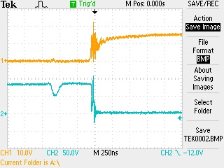
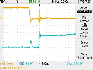
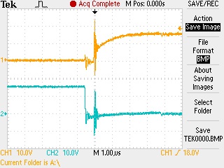
Snubbers are needed, if transient overvoltages become dangerous for the involved devices, or to reduce interference emissions. They will rarely reduce semiconductor losses but add some losses on their own. In a good, low inductance H-bridge design, snubbers should be superfluous.
 
Having the schottkies across the gate drive resistors is working - giving you a speedier turn off - good for reducing losses. Looking at the Vce waveforms it appears that your gate drive signals (at the original source) are a bit unusual - then seem to be putting a short turn on pulse to the IGBT a little before the real turn on pulse - this can be seen in the dip in the Vce before the device switches on properly - it may be that if you have a very spread out circuit there is intereference from the power stage getting into the circuitry that produces the gate signals (this is quite common for new novice designs) - you need to capture (together) waveforms for one low side device G-E and C-E so we can see any funny business on the gate, Regards, Orson Cart.

p.s. the undershoot on the Vge with the shottkies is good rather than bad - ensures a speedy turn off.

pps; from the heatsink photo it appears that your circuit is very spread out - this will give the ringing on the gate drive (at turn on) that we see in your 'scope captures (win.rar) also as you do not have power decoupling caps from HVDC+ to HVDC- ,right by the IGBT's, you get the ringing on the HVDC supply between switching that can be seen on your 'scope traces too.

High power circuits usually require tight layout and good decoupling to stop interference getting into the control.
 
Last edited:
Regarding snubber circuits: it is very common to use RC and RCD snubbers with IGBTs. Next document explains it very clearly (is a bit old but I think it will help).

http://www.irf.com/technical-info/designtp/tpap-5.pdf

I agree that shoot-through can be the main cause of excessive power loss. The mentioned snubber circuits will reduce dv/dt and provably avoid shoot-through situations
 
Regarding snubber circuits: it is very common to use RC and RCD snubbers with IGBTs.
It's also common that designers don't manage a good power electronics layout, either due to objective restrictions (e.g. form factors, required components) or because they don't know the basics. The linked article says, that snubbers may be necessary to ged rid of dangerous (to the semiconductors) voltage transients, which was also my staement in this regard. But if the H-bridge can be designed in a way, that these transients are avoided, you don't need snubbers. Be sure, that state-of-the-art "green" electronics, that chases for 99.x percent efficiency has to avoid all snubbers containing the letter "R".
 

Dear Experts,
Actually I don't have much power electronics layout experience yet as I am new in this area. The board I designed and am using is for evaluation and development but its obvious that it has serious layout issues. And I can't actually figure out where the basic problem is, and if it could be solved by doing a proper layout design.

I applied schottky diodes parallel to gate resistors which has shortened the gate fall time, increased transients at IGBT Vce. Still, same waveforms and problems continues as you can seefrom the measurements (Vcc=55V rms at this measurements to prevent high transients):

69_1308732619.jpg
30_1308732619.jpg
18_1308732619.jpg
23_1308732619.jpg


Those figures are from the same single high side IGBT, with simultaneous Vge (yellow) and Vce(blue) measurements. Could we say the problem is not the result of the shoot through of gate turn off failure but problem (whatever it is) itself is a reason to shoot through? I think those inapproprate shots before Vce rise and fall while Vce is at high condition are results of the ground bounce occured at IGBT switching edges which effects gate driver optocouplers. And could I overcome this problem only by layout improvement?

ps: I applied more decoupling caps close to IGBT's between Vcc and ground.
 

Worth increasing the turn on gate drive resistors to 330 ohm say (still with the diodes in parallel) , this will give a slower turn on and reduce interference effects and may let the converter operate normally (but with some turn on loss) - Regards, Orson Cart.

(p.s. from the waveforms it appears the current is backwards through the device at turn off - hence the little blip at turn off)

also can you show the 2 low side gate drives on the same screen please (under power) ?
 

There are two points, that I don't understand related to the measurement:
- You previously mentioned, that you don't have isolated probes. How did you measure the high side waveforms?
- The 5 ms/div waveform suggests, that the bus voltage is an unfiltered full wave rectified mains voltage. What's the bus capacitor value?
 

- You previously mentioned, that you don't have isolated probes. How did you measure the high side waveforms?
Those are from a single high side IGBT Vge and Vce waveforms. Their reference points are same. I can't measure points simultaneously with different references.
- The 5 ms/div waveform suggests, that the bus voltage is an unfiltered full wave rectified mains voltage. What's the bus capacitor value?
Vcc bus capacitors are 3x5uF = 15uf.
43_1308810783.jpg

Is series inductor after diode bridge necessary? If so, what would its value and important parameters be?

---------- Post added at 08:48 ---------- Previous post was at 08:39 ----------

I agree that shoot-through can be the main cause of excessive power loss. The mentioned snubber circuits will reduce dv/dt and provably avoid shoot-through situations
I will aslo try snubbers to avoid this shoot through situation and feedback soon
 

Dear Orson,
Increasing gate resistor actually don't help. Here the figures are same although gate resistors are 220ohm(with the schottky diodes in parallel). 15V supply somehow is effected by switching noise and that noise couldn't be eleminated by providing slower rise and fall edges for IGBTs. Although I increase the gate resistor value, Vce rise and fall edges seems still sharp about untill half of the Vcc applied and this is not changed with resistor value. I think that sharp edge is enough to effect 15V supply, causing unwanted increase above the threshold voltage of the IGBTs and finally causing shoot through.

Vge1 and Vce1 are same low side IGBT waveforms
Vce2 other low side IGBT waveform
(both are simultaneous measurements as their reference points are same.)

94_1308826326.jpg
2_1308826326.jpg


Here are the low side IGBT Vge's:

25_1308826992.jpg
22_1308826992.jpg
 

The fact, that the turn-on oscillations seem to increase with slower gate drive suggests, that the problem is mainly caused by inappropriate circuit layout, particularly parasitic couplings of output current to the driver circuit.

This refers to the doubts about a "very spread out" circuit, that Orson mentioned in post #22. Perhaps, you should show the missing lower halve of the photo in post #17 or a PCB layout for better understanding.
 

Hi Erhan,
interesting application ;-) hre some questions and some ideas...


The spikes we see low_15v.BMP and high_15v.BMP may very likely come from a "standard improvable measurement setup" with a scope (long GND-wire!! ;-) (Better wind non isolated cable to the GND tab directly at the scope-tip and contact the GND. Use app 10cm wire, wind it to the GND-connection at the measurement tip and use 2cm for connection to the GND pad... try it and check the differenct at this application to the standard 10cm GND straight wire, you will be surprised!)

If the film/ceramic caps at each driver buffer are in the range of 100n and you have an additional 2µ2 ceramic close to each driver there will be no issue with that.
So I assume that the 15V supply is really no big issue.

The next topic... dead time...
If your opinion is: dead time is sufficient... fine. Better you double check to be sure, be so kind.

In the pictures at post #25 we clearly can see (Pic 2,3,4), that you have a deadtime of app 600ns AND that the other switch which should be
"off" at that time is being switched "on" for app 150ns.
This will happen if the driver is not low impedanct enough. It could be, that
1. the resistance is too high (so the schottky will help;-)
2. the wire is not drilled and/or too long
3. the switching is too fast in total
Try to minimize that parasitics. You could try to have app 1..3µs as switching time, but do change the dead time, too.
If all this points will not help, you can go to -5..-10V as "off" level. Than the couppled energy will not have the opportunity to increase the "of" level in the range of the "turn-on" level.

But in addition... maybe the supply voltage is NOT stable enough, too
How long is the wire between DC-link cap and H-Bridge?
How high is the voltage drop on the wires if the cap is fully charged if you measure DIRECTLY
1. at the cap +/-(without load current!)
2. at the H-bridge top and bottom WITH load current??
by the way... DIRECTLY means not 1cm, it means directly!
I strongly recomend the wire length as small as possible means <5cm for each cable. If you have the possibility use several smaller
wires in parallel to reduce the inductance, ok? In addition you should have several µF in parallel to the electrolytic caps.

Good luck

Volker
 

There does appear to be plenty of dead time if the high side gate drives are behaving themselves, the large amount of noise at turn on must therefore be due to layout (i.e. gate drive signal wires being run near output wires etc...) It is very odd that using larger turn on resistors for the gate drive does not quiten things down a bit. Regards, Orson Cart.

It might be worthwhile finding another isolated IGBT driver IC to drive the upper igbt's, one with good immunity to common mode transients, as at the moment when a lower device turns on it pulls down the upper igbt Emitter and a capacitive current can flow through the opto driver possibly partially turning on the upper device as the lower one turns on.
 
Last edited:

As I stated before my layout is a novice one, I don't know you can figure out from the layout picture but you can see it is attached. All the components are used as through hole as this is our capability to mount. I added TVSes,schottky diodes as seen in schematic but they are not included in this layout. I also added decoupling capacitor 5uf right at bottom of IGBT's between VCC and PWR_GND.

Optocouplers are far away from the IGBT's so gate rails are also long and I think that's a bad layout brought out of your feedbacks, where gate rails must be short. This power board layout doesn't include microcontroller which is the source of PWM. It is connected with 20cm wires to the connector at the bottom of the layout (DGND - H1 - H2 - L1 - L2). There where fuses at emmiters of IGBT's for precaution but I removed them and added 0.02ohm resistors. IGBT's are at right side. At the top you can see VCC bus and at bottom its return path PWR_GND.

I hope you can briefly understand the component settlement.

Do you suggest me to change only layout or both layout and IGBT drivers? I choosed those drivers as they are easy to apply and does both drive and isolation. If I use a common gate driver IC, I also need to use pulse transformer in order to do the isolation between microcontroller and power levels.

Volker,
Thanks for your valuable advices, I'll try them. Here are answers for you,
I don't use ceramic but I think they are polyester through hole capacitors both at Vcc and 15V supply rails.
I think I don't have dead time issues. The time delay between signals are enough and nothing changes when I increase and decrease the dead time ofcourse between safe area (I apply at least 240ns at most 1us)
IGBT's and gate drivers are both really fast. I choosed them intentionally that fast to do the switching fast and get rid of much switching loss. I think 1..3us switching time is too slow for this IGBTs and would lead to much switching loss. I think gate signal path is too long. I hope I could overcome them with new layout.
I can see much of your concern is also about weak layout. Please see the layout for several of your questions.

I will post new layout here soon for you to check if there are still weak areas.
 

Attachments

  • layout.jpg
    layout.jpg
    1.8 MB · Views: 93

OK - the fact that the gate drive 0V (emitter connection) lines share tracks with the power lines may be a big part of the problem - better to take a twisted pair direct from the driver o/p to the G-E of the igbt, generally the lengths mentioned for connections seem a bit long for successful converter operation, Orson Cart.
 

Vge1 and Vce1 are same low side IGBT waveforms
Vce2 other low side IGBT waveform
(both are simultaneous measurements as their reference points are same.)

94_1308826326.jpg
2_1308826326.jpg


Here are the low side IGBT Vge's:

25_1308826992.jpg
22_1308826992.jpg
Okay so you've finally provided some waveforms ALMOST showing what I wanted. I am not convinced this simply a layout issue. I think that the gate resistors may be too high, which allows the gate voltages to be "pulled" on by the gate-drain capacitance of each fet during switching. This is a common cause of slow switching speed and oscillation. Your dead time looks very large already, so I doubt that is a problem.

Here's what you should do. Probe the Vge and Vce of each FET during the switching transient of its drain (not its gate). Zoom way in so you can clearly see any high frequency ringing (like 50ns/div). If the ringing on the two waveforms is similar in shape, then that means your Cdg is the issue.
 

I think that the gate resistors may be too high, which allows the gate voltages to be "pulled" on by the gate-drain capacitance of each fet during switching.
Please review the previous discussion related to this point. The final setup (not shown in the layout) uses an asymmetric R/RD combination, it should avoid Cdg feedback effects.
 

Please review the previous discussion related to this point. The final setup (not shown in the layout) uses an asymmetric R/RD combination, it should avoid Cdg feedback effects.
Cgd can happen at both turn on and turn off, so the diode won't always help.

Also the R/RD technique is meant to add dead time, so what's the point of using it when he already has dead time built into the PWM? If you want to speed up switching, just lower the gate resistor, no diodes needed.
 

As FvM said, we tried to overcome that oscillation problem by an asymmetric R/RD combination. I applied 10ohm to 220ohm different gate resistances with different dead times. Currently I have 47 ohms gate resistance at turn on and at turn off a schottky and again 47 ohms series to it, which will bring out about 47//47 = 23ohms at gate off time. Also tried schottky without any series resistor to it but the problem still occurs. So we finally decided the problem is caused by weak layout design.

So while I am doing a new layout design, could you experts please give some advices which I must take care of? Please see my previous layout and tell me its weaknesses.

Thanks

---------- Post added at 18:45 ---------- Previous post was at 18:43 ----------

If you want to speed up switching, just lower the gate resistor, no diodes needed.

I started with only 10 ohm resistors at gate with no diode. Even that configuration oscillated :(
 

I started with only 10 ohm resistors at gate with no diode. Even that configuration oscillated :(
But you haven't shown us the oscillation in enough detail to say why it's oscillating. All we see is a bunch of awful noise. You need find where that RF current is actually flowing to solve the problem.

I've solved issues like this before by adding gate capacitance to the FETs, which mitigates the effect of Cdg capacitance on gate voltage. Then I'll just have to decrease Rg to get fast switching times. It takes more power from the gate drivers, but that's generally not a concern.

I still think reverse recovery in your switch diodes may be the culprit as well. Are you using the body diodes of the IGBTs, or external diodes?

I actually don't know why it is oscillating. My prediction is the switching noise of IGBT's couple with the driver.
I tried 2.2nf extra gate capacitance while having 220 ohm gate resistance with parallel diode. I increased dead time to 1.5us. That made the Vce even worse.
The IGBTs doesn't include body diodes. I tried two different body diodes while one of them has max of 105ns recovery time.
 
Last edited:

Status
Not open for further replies.

Similar threads

Part and Inventory Search

Welcome to EDABoard.com

Sponsor

Back
Top