Continue to Site

Welcome to EDAboard.com

Welcome to our site! EDAboard.com is an international Electronics Discussion Forum focused on EDA software, circuits, schematics, books, theory, papers, asic, pld, 8051, DSP, Network, RF, Analog Design, PCB, Service Manuals... and a whole lot more! To participate you need to register. Registration is free. Click here to register now.

IGBT switching loss control

Status
Not open for further replies.
Please find some answers to your remarks.
[...]
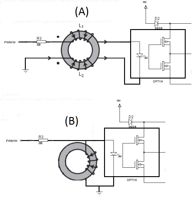
Optocouplers are far away from the IGBT's so gate rails are also long [...]
###Please try to use drilles wires instead, 2drilles wires per IGBT.
[...]
Do you suggest me to change only layout or both layout and IGBT drivers? I choosed those drivers as they are easy to apply and does both drive and isolation. If I use a common gate driver IC, I also need to use pulse transformer in order to do the isolation between microcontroller and power levels.
###first lets find the weak point, currently we have too less details
[...]
I don't use ceramic but I think they are polyester through hole capacitors both at Vcc and 15V supply rails.
###Polyester is fine for the moment

I think I don't have dead time issues. The time delay between signals are enough and nothing changes when I increase and decrease the dead time ofcourse between safe area (I apply at least 240ns at most 1us)
IGBT's and gate drivers are both really fast. I choosed them intentionally that fast to do the switching fast and get rid of much switching loss. I think 1..3us switching time is too slow for this IGBTs and would lead to much switching loss. I think gate signal path is too long. I hope I could overcome them with new layout.
###right, but please DO try reducing the switching speed with less current to make sure that this is not the issue. To close this topic finally please start with app 4R7Ohm as gate resistor, continue with 10R, 15R, 22R. 47R. 100R. 150R. 220R and do measure and compare the length of the oscillation and the 200ns "hills" in the switching processes which can be seen on the 2 upper pictures.

Than add a 220µf Elko to each Driver, make sure that the polyester is changed to a 2µ2..4µ7 Kerko with shortest wires to the driver directly and compare with 2..3 Resistor values.

Than add >33mF consisting out of 5..10 paralleled Electrolytics which are mounted with max 5cm thick wire over the H-bridge and tell us the difference in switching and disturbance

This above will help to reduce the possible issues...
I am very curious to your results
 

A quick look at the diode data sheet shows that there will be some noise generated if you try and force these off too fast (by turning the igbt's on fast), for me, I would say the biggest contributor is likely to be a small pulse of current though the upper gate drive opto's when the lower device in the string turns on - this would account for the extra heat mentioned (due to the shoot thru on the power rail) and the RF noise evident - you could make a common mode block by taking the two wires than run to the opto LED and winding them on a small - med sized power toroid (5 turns say) - and do this for both high side drives - if this improves matters then the opto drivers are to blame. You can put the toroid on the 2 wires that run to the GE if easier (bifilar as don't wan't any differential inductance). Do you have the part number for the opto diver please? Regards, Orson Cart.

p.s. The igbt's you are using do not have internal diodes - and there are no reverse diodes shown in the hardware photo - please confirm that you have had such diodes in place for all the testing..!!!
 
Last edited:

Dear Orson,
Would you please clarify what body diode important parameters should be? I have body diodes for each IGBT soldered to wires at bottom side, that's why they are not seen at layout and photo. I also used slower version body diodes and that made no change. Still body diodes won't be an issue because I also applied slower IGBTs with internal diodes and have the same issues.

As you mentioned I strongly think I have same time switching on problem of the same string IGBTs leading to shoot through. And I want to be sure and overcome this problem by some modifications on this layout and change it after finding the root of the problem. Please see the figures, I think you want me to have connection A. Am I right?


Optocoupler.
 

Connection A correct, bifilar preferable rather than seperating the windings, the data sheet for the opto driver looks good for common mode - but the 1pF capacitance can still upset the drive for high dv/dt on the high side emitters (300V in 20nS gives 15mA total on the LED drive lines) so it won't hurt to add the CM choke (both high sides) and check.
diodes across the igbt's should be ultra-fast, else the reverse currents and loose layout will affect the control.
Make sure you are putting at least 16mA into the opto LED's. Pins 1 & 4 should be connected to pin 3 (0 volt on the opto led) - Regards, Orson Cart.
 
Last edited:

how many volts is the uP o/p? if it is 5V less 1.5 volts on the opto led gives 3.5 volt drive across 220 ohm = 15.9mA, for 3.3v uP, the drive current will be (3.3-1.5)/220 = 8.2mA, Regards Orson Cart.
 
Last edited:

It is 3.3V. I know the recommended input current is 10mA-16mA. But I want to drive two IGBT's with one uc output. The driver is good with 8mA as this is the minimum allowed input current. Hence, temporarily I have 180ohms right now.
 

I didn't do that configuration yet but after solving this problem, my intention is to drive 2 optos with one uc pwm output. the 220ohm resistors should be parallel to each other. I mean leds should be parallel.
 

my intention is to drive 2 optos with one uc pwm output. the 220ohm resistors should be parallel to each other.
Strictly spoken, 16 mA output current won't be guaranteed by the specification of most uC port pins, even 10 mA is questionable. 2x16 mA would be clearly beyond rated currents. So an driver transistor is absolutely required for the parallel circuit but also advisable for the single output.
 

I didn't do that configuration yet but after solving this problem, my intention is to drive 2 optos with one uc pwm output. the 220ohm resistors should be parallel to each other. I mean leds should be parallel.
You have to ensure the LEDs are getting about the same current, so you need to either drive them in series, or give each of them their own series resistor. Putting them directly in parallel with one series resistor is a bad idea.
 

That's I was talking about.
Okay, I wasn't sure.

At this point you should really try to get some differential scope probes. It seems likely that you're dealing with some common mode signal phenomenon, which normal scope probes won't be able to show correctly. Also some kind of wideband current transformer of current probe would be very useful.
 

Here my last configuration measurements. I changed the IGBT's with slower ones. Gate resistors are 22ohm with parallel schottky diodes. I think different dead times with this configuration outputs interesting results. (Or maybe I think so) Please see the zipped waveforms. The measurements are simultaneous low side IGBT Vge and Vce voltages. When I have 240ns dead time the Vge and Vce (named as Vge_rise,Vge_falls,Vce_lowsides,Vce_lowsides_wide) seems good. Though Vce_lowsides shows there is a shoot through because of the fall time tails are long. When I increase the dead time to prevet this problem to 300ns,400ns... the Vce signals start to change to the ones like my previous posts. Could this be a known issue?

Could the optocoupler output impedances be my main problem? As they may be very high for this application. How can I be aware of that?
 

Attachments

  • deadtime_waveforms.rar
    21 KB · Views: 59
Last edited:

300nS looks best at this load, we still need to see a low side gate together with the collector to get a good idea of how things are behaving - how is the temp rise now? please list the devices you are using, igbt and diode. Regards, Orson Cart.
 

I only tried this configuration till 1A with a smaller passive cooler without fan but still I can feel the temprature rise on the cooler. Although I increase the dead time, I can't get rid of shoot through. When dead time is smaller than 300ns yes the waveforms seems regular but dead time seems insufficient. When I increase the dead time, waveform starts to become bad. In each configuration it heats up much.
The IGBT(IXDH30N120D1) has internal recovery diode.
 

And please have a quick look at my new layout design, and suggest if it has weak places. I highlighted the important parts on one IGBT area, the others are nearly same.

I kept the ground connections of driver optocouplers with IGBT emmiters intentionally thin in order to decrease switching coupling. I tried to keep gate drivers as close to IGBTs as possible. The gate drivers are 30mm away from the IGBT's. Between them stands TVS diodes and gate drive resistors with schottky. In my previous design the distance between them was more than 60mm.

newlayout.jpg
 

I kept the ground connections of driver optocouplers with IGBT emmiters intentionally thin in order to decrease switching coupling.
You want that trace to be as short and wide as possible. You want to keep the loop formed by the bootstrap capacitor, driver output, gate RD network, IGBT gate emitter, and driver ground return, as small as possible.

Here's a picture showing the loop in red:
gateloop.PNG
and I tried to keep gate drivers as close to IGBTs as possible. The gate drivers are 30mm away from the IGBT's.
Try for 15mm. I think it's doable even with big through hole components.
Between them stands TVS diodes and gate drive resistors with schottky.
You want the TVS diodes to be as close as possible to what they need to protect (the IGBT gates, right?).
 
have you got the common mode (CM) blocking chokes in the high side gate gate drives? (to the opto led)

Regards, Orson Cart.
 
Last edited:

yes Orson, I have them ...

mtwieg,
the TVS diodes are to protect the optocouplers not the gate.

---------- Post added at 11:48 ---------- Previous post was at 11:25 ----------

I actually don't understand the waveforms I posted last ( deadtime_waveforms.rar‎) Although I increase the gate drive dead times (and yes I can see all four gate signals simultaneously while I don't drain current from the collectors of IGBT's and waveforms are fine) I can't have dead time at collector voltages when I start draining current. When I investigate two low side IGBT Vge and Vce's although there is a dead time between gate voltages, there is no dead time between collector voltages and this never changes though I increase or decrease the dead time. I think that's my main problem of overheating. Any suggestions for this problem?
 

Status
Not open for further replies.

Similar threads

Part and Inventory Search

Welcome to EDABoard.com

Sponsor

Back
Top