AllenD
Member level 5
Hi
I recently got my TSMC 65 nm IC back. I am trying to wirebonding it to my PCB. Can I please ask a few rookie questions?
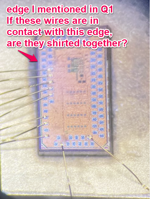
1. I have a ring-like edge surrounding my IC core. I assume it is the guard ring layer I added in the end before my tapeout due date... Is that edge conductive? Meaning If the wirebonding wires are in contact with the edge, would they short together?
2. Are the IO pad protected by a layer of insulator, which would be destroyed by wirebonding wedge? In other words, if I just land a gold wire on top of an IO pad without wirebonding wedge to smash it on the pad, is it still connected? Or the wirebonding wedge is needed to smash the gold wire to create connection to conduct current?
Thanks