Continue to Site

Welcome to EDAboard.com

Welcome to our site! EDAboard.com is an international Electronics Discussion Forum focused on EDA software, circuits, schematics, books, theory, papers, asic, pld, 8051, DSP, Network, RF, Analog Design, PCB, Service Manuals... and a whole lot more! To participate you need to register. Registration is free. Click here to register now.

[SOLVED] i want to optimize this PCB using EAGLE

Status
Not open for further replies.

Qwme5

Junior Member level 2
Joined
Jan 19, 2011
Messages
23
Helped
0
Reputation
0
Reaction score
0
Trophy points
1,281
Activity points
1,444
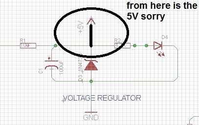
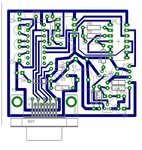
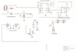
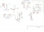
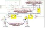
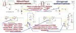
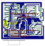
Hi am new in designing any kind of PCB i start my design using eagle 5.11.0 i draw the circuit diagram without any problem my problem is i cant draw the pcb correctly i uploaded both of the circuit diagram and PCB diagram its kinda messy so i need ur help to minimize the no of jumpers and optimize the overall schemeView attachment schemet.rar
 

See this example:


By the way, use only one resistor for R3&R4… :-D
 

Attachments

  • sch.ver2 a.rar
    16.1 KB · Views: 74
Last edited:
You can always readjust some wiring. :smile:
And maybe it’s better to have a capacitor connected to GND at pin5 of the U4. A standard value between 10nF and 22nF. See the modified diagram.
 

Attachments

  • Schematic_v3a.pdf
    30.8 KB · Views: 102
  • sch ver3.rar
    16.3 KB · Views: 68
It would be worthwhile running the ERC on the schematic & DRC on the layout.

Orhtogonal lines for wires make schematics easier to read.

Personally I prefer to make explicit power connections to ICs so I would invoke the power connections of U2 and connect them to power & ground.

Keith.
 
  • Like
Reactions: Qwme5

    Qwme5

    Points: 2
    Helpful Answer Positive Rating
On the other hand, I have started to play only for 5 minutes, but for a good layout need more time to spend, and it’s more difficult to rearrange someone project, maybe for a small schematic like this it’s better to start from the scratch, also because some of the capacitors packages need to be changed in order to accept large volume for. That’s a job to do in many steps, with lot of patience and multiple versions on the run. :cool:


**broken link removed**
 

Attachments

  • schematics v4.rar
    50.3 KB · Views: 86
Last edited:
I think the problem with the original layout (other than the tracks were far too thin) was the component placement. As mister_rf has done, re-arranging the components makes the routing far better.

Keith.
 
  • Like
Reactions: Qwme5

    Qwme5

    Points: 2
    Helpful Answer Positive Rating
Working in small steps you can squeeze the layout, see:
 

Attachments

  • Small layout.pdf
    121.4 KB · Views: 115
  • schematics v5.rar
    16.2 KB · Views: 79
Last edited:
guys i really dont know what to say thank u very much specially mister_rf i cant found any word to express my gratitude to u

i am right working in the last board u have upload it to me which is V5

thanks alot all of u

My Regards

---------- Post added at 00:35 ---------- Previous post was at 00:23 ----------

after checking the board it seems that u forget to connect the 5V to the RS232 and the Monostable

---------- Post added at 00:39 ---------- Previous post was at 00:35 ----------

67_1311784728.jpg
 

There is an airwire on Q1 base but 5V seems connected.

As I mentioned before, you really need to run the ERC on the schematic - it would point out the drawing errors you have.

You also have some unnecessary junctions in quite a few places - round Q1, Q2, D6, D7, U2C, R2 & D4.

Keith.
 
  • Like
Reactions: Qwme5

    Qwme5

    Points: 2
    Helpful Answer Positive Rating
It’s not my mistake… ;-) Yes, I didn’t check all details, but you forgot to put in in the first place. Anyway, give me some minutes, I’ll do all necessary corrections. If you are happy with this just press ''thumbs up'' button. :-D
 
  • Like
Reactions: Qwme5

    Qwme5

    Points: 2
    Helpful Answer Positive Rating
i really dont know what to say thank u verrrry much all of u guys
 

So, and a final version, not the best, only the latest release. For any problems you get your money back. :-D
 

Attachments

  • schematics ver7.rar
    44.7 KB · Views: 70
  • schematics 7.JPG
    schematics 7.JPG
    212.7 KB · Views: 98
  • Like
Reactions: Qwme5 and FvM

    FvM

    Points: 2
    Helpful Answer Positive Rating

    Qwme5

    Points: 2
    Helpful Answer Positive Rating
sorry mister_rf i found another mistakes and i correct them all now am doing the board again can u take a look and tell how am going till now
 

Attachments

  • Desktop.rar
    16.3 KB · Views: 64

mmm i have connect almost everything but there still some wires i dont know how to connect them can u plz see this board
 

Attachments

  • V7.rar
    10.8 KB · Views: 77

Let’s see what are ‘’the problems’’ in the modified schematics.

  1. Need to have this capacitor, If you don’t want it, simply don’t use it.
  2. I have changed only order of the gates, no problem of the design functionality.
  3. I have changed the package for this capacitor
 

Attachments

  • original schematics.JPG
    original schematics.JPG
    132.1 KB · Views: 140
  • modified schematics.JPG
    modified schematics.JPG
    130.6 KB · Views: 98
  • Compare 1.JPG
    Compare 1.JPG
    119 KB · Views: 93
Last edited:
  • Like
Reactions: Qwme5

    Qwme5

    Points: 2
    Helpful Answer Positive Rating
4. No need for R3, R3||R4, so use only R4, you can choose later the correct value
5. Not important if R2D4 connected to ‘’12V’’ instead of ‘’5V’’.
6. Not important if R8 connected to the 12V instead to the 5V power supply.
 

Attachments

  • compare 2.jpg
    compare 2.jpg
    195.3 KB · Views: 97
  • Like
Reactions: Qwme5

    Qwme5

    Points: 2
    Helpful Answer Positive Rating
And in my opinion you may need to use an external power supply, so I have placed just in case an external board connector plus one diode. See the PCB board attached.
 

Attachments

  • Extra Power supply.JPG
    Extra Power supply.JPG
    397.3 KB · Views: 109
  • Board extra power.rar
    6.9 KB · Views: 122
  • Like
Reactions: Qwme5

    Qwme5

    Points: 2
    Helpful Answer Positive Rating
Mister_rf i really cant find the appropriate words to thank u
thank u very much u helped me so much
 

By the way in this application, try to replace 1N4001 series diodes with some fast switching diodes series like BA157/BA159/ UF1001/UF1002/UF4002/UF4004 or some schottky diodes.
 
  • Like
Reactions: Qwme5

    Qwme5

    Points: 2
    Helpful Answer Positive Rating
i have one another question right now am working on another project and i want to make a double layer PCB using eagle how can i do this
 

Status
Not open for further replies.

Part and Inventory Search

Welcome to EDABoard.com

Sponsor

Back
Top