Venkadesh_M
Advanced Member level 4
- Joined
- Jun 26, 2013
- Messages
- 1,374
- Helped
- 258
- Reputation
- 516
- Reaction score
- 254
- Trophy points
- 1,363
- Location
- Coimbatore, India
- Activity points
- 8,019
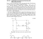
Here is its block diagram they are leveling up but still taking Ho from Vb can not understand.....