Continue to Site

Welcome to EDAboard.com

Welcome to our site! EDAboard.com is an international Electronics Discussion Forum focused on EDA software, circuits, schematics, books, theory, papers, asic, pld, 8051, DSP, Network, RF, Analog Design, PCB, Service Manuals... and a whole lot more! To participate you need to register. Registration is free. Click here to register now.

How to get through the problem related to MOSFET Switching?

Status
Not open for further replies.

SACHIN C

Full Member level 2
Full Member level 2
Joined
Jul 6, 2013
Messages
143
Helped
4
Reputation
8
Reaction score
4
Trophy points
18
Visit site
Activity points
1,048
Dear All,
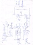
Pls guide me to get thru the problem related to MOSFET Switching.
Mosfet using K62j60W(Max. 600V/61.8A)

Driver used is TD350E which is able to source 0.75A other then 25c.
But,Mosfet needs 1.5A @ full load.Since presently am testing for at no load,the gate waveform shows On/OFF behaviour near falling edge.
Push -Pull Transiter used are TIP122 & TIP127 with base resistor as 33K(as HFE is 3500) & collector resistor used is 33ohms.

Mosfet Gate resistor used is 10ohm,gate to source resistor used is 10Kohm.


Supply used for Collector & Driver is 15V made from 7815(for no load testing as it is not able to deliver current for full load which is 1.5A in our case).


Thanks & waiting for valuable help.....:)
 

Attachments

  • Driver Circuit.jpeg
    Driver Circuit.jpeg
    542.1 KB · Views: 351
Last edited:

You're not very clear on what your problem actually is...

But those 33K resistors on the pushpull drivers will slow you down a lot. The resistance should be much lower, probably around 100ohms. And you should eliminate those 33ohm resistors on the collectors of the tip122.

Also I can't understand how your power supply for the high side drivers is supposed to work...
 

yeap that is the datasheet for mention MOSFET

- - - Updated - - -

mtwieg

Actually i am observing Waveform at the GATE as shown in above attached file,so my query is whether selected Rgs,Rg are correct?
Also the TIP122 & TIP127 series is darlington so its gain is almost 3500 for Ic 1.5 A,Rb comes around 33K,but i used 4.7K as derived follows,so Rbase & R base-source resistor are correct?
Hfe=3500
Hfe=Ic/Ib
Ib=1.5/3500
Ib=0.428mA
Vbe=(Vb-0.7)/IbRb
(15-0.7)/0.428m=Rb
Rb=33.41Kohm
Rb=1/3=33.41Kohm/3=11.13Kohm(1/3 don't know the reason but,got thru some online site)
Correct me if i am mistaken,

If possible help me for resistor selection?
Presently collector 33ohm resistor is removed from the circuit as 10ohms is available for current limit in MOSFET GATE path


Thanks & waiting for valuable feedback,:)
 

I think he meant that your transistors' capacitances make slow RC time-constants, with the 33k resistors. So you would need to lower the 33k, to get fast-enough edges to switch the MOSFETs very well. Maybe you could lower the signal amplitude, before the darlington inputs. Or use some other transistors.
 

tgootee,
Yes i got the point,but what should be the lower value for TIP122 & TIP127 base resistor for 1.5A Collector current pls guide me & for Gate Resitor?:-?

Thanks & waiting for valuable support,:)

- - - Updated - - -

Dear All,
Also provide me some guidance for MOSFET Snubber calculation ?
Heat Sink Area calculation for Thermal Resistance of 0.328C/W with 102W Power Dissipation?
MOSFET Rg & Rgs selection?
Transistor Push-Pull(TIP122 & TIP127) Rb & Rbs selection?

Thanks & Waiting for valuable support,:smile:

- - - Updated - - -

Dear All,
Also provide me some guidance for MOSFET Snubber calculation ?
Heat Sink Area calculation for Thermal Resistance of 0.328C/W with 102W Power Dissipation?
MOSFET Rg & Rgs selection?
Transistor Push-Pull(TIP122 & TIP127) Rb & Rbs selection?

Thanks & Waiting for valuable support,
 

Pls guide me to get thru the problem related to MOSFET Switching

Dear All,
Also provide me some guidance for MOSFET Snubber calculation ?
Heat Sink Area calculation for Thermal Resistance of 0.328C/W with 102W Power Dissipation?
MOSFET Rg & Rgs selection?
Transistor Push-Pull(TIP122 & TIP127) Rb & Rbs selection?

Thanks & Waiting for valuable support,:smile:
 

Determining Optimal Snubber Components:

1. Measure the frequency, f, of the resonance or ringing.

2. Add a shunt capacitor and adjust the value of this temporary capacitor until the frequency of the ringing is reduced by a factor of two. I've left out the math but the value of this resulting capacitor will be three times (3X) the value of the parasitic capacitance, C, that is creating the resonance. Remove the temporary shunt capacitor.

3. Because the parasitic capacitance is now known, the parasitic inductance can be determined using the formula:

L = 1 / [ (2πf)² · C ]

where f = (the original) resonant frequency from step 1, and C = the parasitic capacitance that was determined in step 2.

4. Now that both the parasitic capacitance and inductance are known, the
Characteristic Impedance, Z, of the resonant circuit can be determined using the following formula:

Z = √(L / C)

i.e. the square root of the quantity L divided by C,

where L = parasitic inductance and C = parasitic capacitance.

5. The resistor value used for the for the RC snubber network should be equal to Z, the value of the characteristic impedance, and the capacitor, if used, should be sized between four and ten times the parasitic capacitance. The use of larger (than 4X) capacitors slightly reduces the voltage overshoot at the expense of greater power dissipation in the resistor.
 
tgootee,
Thanks for help,but the resistor required will be CFR or MFR?
Normally preffered is CFR but, reason?
i came accross the online calculation where they are saying below mention calculations;is this will also work?
Snubber Resistor Rs=Vo/Io(Vtg when Switch is open & Current when Switch is switching from ON to Off)
Power Dissipation=(1\2)C(V)^2f,
Assuming power dissipation of 2W,we need to calculate for Snubber Capacitor & f =Switching Frequency,


Thanks & waiting for valuable support,:smile:
 

Shall we need to use Snubber capacitor always non-polarity one for MOSFET?

Thanks,:smile:
 

Dear all,
can we use only Capacitor as an snubber instead of RC or RCD(Half Bridge MOSFET)?
Also,what type of capacitor need to be used & why?
Why not Electrolytic?

Thanks & waiting for enhancement of knowledge,:smile:
 

Dear All,
Snubber i have used is C=10nF/630V,R=22ohm/0.25W According to above calculation
The Drain to Source for Half Bridge MOSFET provided is through Dimmer Via 4700uF/450VDC(2 capacitor in series) which itself capacitor act as an filter capacitor but as i am increasing the Voltage beyond 50VDC the dimmer current crosses 3A,the testing is without load.I think the huge capacitor takes current but i am observing shoot at the Drain shall i need to slow the gate by reducing gate resistor which is 11ohm currently.
Also,Push-Pull cuircuit Base resistor is 2.7K & Base to Collector resistor is 2.7K shall i need to change this resistor also to slow down the dv/dt rate for drain to source
Also the snubber resistor is of low wattage it need to be change but,for no load testing i am using it later on i will change it


Thanks & waiting for support to enhance the knowledge,:smile:
 

If you just a capacitor then it will charged in the first moment of the spike itself and there will be no more protection for dv/dt, And also it will allow the spike to apply on the load..
 
A good designed half-bridge or bridge inverter doesn't need snubbers. They might be necessary, if you are unable to reduce the circuit inductance that causes oscillations, and the oscillations either are at risk to exceed the transistor voltage rating or EMC limit values. But snubbers always cause additional losses.

So the primary design objective is in reducing circuit inductance. Bus capacitors are important in this regard. (Additional low inductance bus capacitors are sometimes designated as "snubber capacitors", but they have nothing to do with lossy RC or RCD snubbers damping oscillations at the switching nodes).
 
(Additional low inductance bus capacitors are sometimes designated as "snubber capacitors", but they have nothing to do with lossy RC or RCD snubbers damping oscillations at the switching nodes).
True!!!

Sachin, I suggest you give a look at this AN:
https://www.fairchildsemi.com/an/AN/AN-6076.pdf
I found it very interesting some time ago.
 
Dear All,
i have used 7815 as an Bootstrap Supply with Diode & 4.4uF/63VDC capacitor as an input & 10uF/63VDC as an output capacitor,it is providing 15v at the Gate but whenever i am trying to increase the Vdd,Output Waveform & Gate waveform for Higher Side shows shoot & noisy effect(Lower Mosfet Gate shows less shoot negligible,but becomes noisy)?

As per attached file for floating supply,
Thanks & waiting for support to enhance the knowledge,:smile:
 

whenever i am trying to increase the Vdd,Output Waveform & Gate waveform for Higher Side shows shoot & noisy effect
This is a very common issue in SMPS designs. I blew up tens of MOSFETs trying to make them working properly...
This is a thread I posted some months ago:

https://www.edaboard.com/threads/280785/

From the best of my knowledge, I think you should review the board design: reduce track lengths to minimise parasitic inductances and avoid coupling between high-impedance nets.

Cheers!
 

Rik797,
How did your problem got solved?
Also i reduced track length to its maximum extend,also the Bus Link Capacitor Are near to Switches,

Thanks & waiting for support to enhance the knowledge,:smile:

- - - Updated - - -

- - - Updated - - -

Dear All,
If we are using Transistor Push-Pull(NPN-PNP) Circuit in between Driver & Mosfet to drive high current Mosfet do we need gate to Source resistor as for Transistor Base to Collector is also used?


Thanks & waiting for support to enhance the knowledge,:smile:

- - - Updated - - -
 

I also employed 4.7-ohm resistors between the drives and the gates.
I don't think a resistance between gate and source terminals is necessary.
I forgot mentioning that ground loops must also be avoided!!!
 

Status
Not open for further replies.

Similar threads

Part and Inventory Search

Welcome to EDABoard.com

Sponsor

Back
Top