Continue to Site

Welcome to EDAboard.com

Welcome to our site! EDAboard.com is an international Electronics Discussion Forum focused on EDA software, circuits, schematics, books, theory, papers, asic, pld, 8051, DSP, Network, RF, Analog Design, PCB, Service Manuals... and a whole lot more! To participate you need to register. Registration is free. Click here to register now.

How to design an ADC circuit with an external sampled signal

Status
Not open for further replies.

nadd

Member level 1
Joined
Oct 3, 2022
Messages
33
Helped
0
Reputation
0
Reaction score
0
Trophy points
6
Activity points
322
Hi everyone,

I'm very new to designing a circuit. So, I need some help.

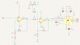
I need to design an ADC for an external, sampled, single-ended signal. The frequency is 1 Mhz, and desired speed is at least 4msps and the resolution is at least 14 bits.
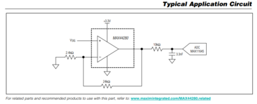
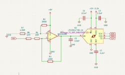
I checked ADC chips and found LTC2314-14 to use. But, LTC2314-14 has inputs for S/H, and my input signal is already sampled. Would it be a problem? (LTC2314-14 Datasheet: https://www.mouser.com/datasheet/2/609/231414fa-2954440.pdf )

Also, I found ADS1605, this one has differential input, so will I need a single-ended to differential converter? (ADS1605 Datasheet: https://www.ti.com/lit/ds/symlink/ads1605.pdf?ts=1664705456913 )

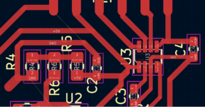
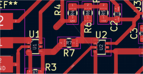
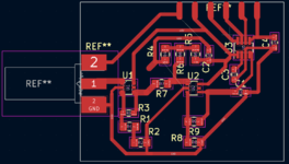
If there are any different ADC chips that you would recommend, please let me know. (Preferably, easy to solder). Also, which additional components should I use in my design?

Thanks in advance!
 

Hi
I changed V(ref) to 5V,
What`s the reason for it?
In the very most cases this reduces system performance. Maybe down to less than 7 bits.
Mind: the performance of an ADC always worse than the performance of it´s REF.
5V supply isn´t a REF at all. It drifts with time, with temperature, with load current and is noisy.
There is a big difference between 5V supply and 5V REF.

One valid reason to use 5V supply as REF could be to have a ratiometric analog input to the ADC.
But still in this case I´d use VREF (or amplified VREF) to supply the ratiometric circuit.

Is there a mistake I made
Oh yes.
Indeed I wonder about this question, because the ADC datasheet provides good informations on how to choose a suitable input amplifier. It even tells some good choices.
Just to avoid that I have to repeat all the datasheet section here, please read it carefully and tell us what you understand and where you need help.

***
Reading datasheets in general:
.. may be annoying. I agree. But is Í see no way around. Every professional designer does it (has to do it).
I guess I step through more than 100 pages of dataseet in average per day. This does not mean I read every word on every page. I rather go through the headline of the chapters ... and focus on the informations I need.
So with increasing experience you need less time to get the expected informaton from the datasheet .. consuming less time.

Back to REF: Here also the datasheet gives good support.

Just to give you a number of what your REF and OPAMP choice will result in:
The datasheet says the ADC can have an ENOB (number of bits you can rely on) of up to 12 Bits up to nyquist.
Your choice may result in maybe 30% of amplitude error at 1MHz (OPAMP GBW) that just leaves you less than 2 reliable bits. This sounds awful .. but it´s worst case ... and it´s becoming better at lower frequencies.

Coosing supply voltage (ST L7805 datasheet) as VRef my result in +/-2% (4% in total) inital voltage error at constant 25°C. Since this can be cancelled out we don´t include it in the ENOB calculation.
So let´s focus on drift: (No worst case "Max" values, just the typical vlues used!)
* Line regulation: 2mV
* Load regulation 25mV
* 40° temperature drift: 44mV
* noise: 50uV RMS .. --> about 300uVpp (I wonder about this low noise)
* long term drift: not specified
* load transients and line transient regulation: realistically on properly bypassed 7805: 5mV (guessed)
added: 78mV
realistically (depends on circuit) you may expect 40mV.
40mV on 5V is a bit less than 1% or a ratio of 1:125.
125 is about 128 which is 2^7. This means there just are about 7bits you can rely on. It´s just a 7 bit ADC performance.
And sadly this does not improve with lower signal frequency.

Conclusion:
* Choosing 5V as VRef reduces ENOB to about 7 bits over the full bandwidth
* choosing your OPAMP reduces ENOB further down below 2 bits at high signal frequencies

Klaus
 
Hi

What`s the reason for it?
In the very most cases this reduces system performance. Maybe down to less than 7 bits.
Mind: the performance of an ADC always worse than the performance of it´s REF.
5V supply isn´t a REF at all. It drifts with time, with temperature, with load current and is noisy.
There is a big difference between 5V supply and 5V REF.

One valid reason to use 5V supply as REF could be to have a ratiometric analog input to the ADC.
But still in this case I´d use VREF (or amplified VREF) to supply the ratiometric circuit.


Oh yes.
Indeed I wonder about this question, because the ADC datasheet provides good informations on how to choose a suitable input amplifier. It even tells some good choices.
Just to avoid that I have to repeat all the datasheet section here, please read it carefully and tell us what you understand and where you need help.

***
Reading datasheets in general:
.. may be annoying. I agree. But is Í see no way around. Every professional designer does it (has to do it).
I guess I step through more than 100 pages of dataseet in average per day. This does not mean I read every word on every page. I rather go through the headline of the chapters ... and focus on the informations I need.
So with increasing experience you need less time to get the expected informaton from the datasheet .. consuming less time.

Back to REF: Here also the datasheet gives good support.

Just to give you a number of what your REF and OPAMP choice will result in:
The datasheet says the ADC can have an ENOB (number of bits you can rely on) of up to 12 Bits up to nyquist.
Your choice may result in maybe 30% of amplitude error at 1MHz (OPAMP GBW) that just leaves you less than 2 reliable bits. This sounds awful .. but it´s worst case ... and it´s becoming better at lower frequencies.

Coosing supply voltage (ST L7805 datasheet) as VRef my result in +/-2% (4% in total) inital voltage error at constant 25°C. Since this can be cancelled out we don´t include it in the ENOB calculation.
So let´s focus on drift: (No worst case "Max" values, just the typical vlues used!)
* Line regulation: 2mV
* Load regulation 25mV
* 40° temperature drift: 44mV
* noise: 50uV RMS .. --> about 300uVpp (I wonder about this low noise)
* long term drift: not specified
* load transients and line transient regulation: realistically on properly bypassed 7805: 5mV (guessed)
added: 78mV
realistically (depends on circuit) you may expect 40mV.
40mV on 5V is a bit less than 1% or a ratio of 1:125.
125 is about 128 which is 2^7. This means there just are about 7bits you can rely on. It´s just a 7 bit ADC performance.
And sadly this does not improve with lower signal frequency.

Conclusion:
* Choosing 5V as VRef reduces ENOB to about 7 bits over the full bandwidth
* choosing your OPAMP reduces ENOB further down below 2 bits at high signal frequencies

Klaus
Hi Klaus,

Thank you very much! And, sorry for the late answer.

I prepared the circuit, but the opamp didn't work properly. It was giving the same signal as the input signal at 1 Hz, almost none at higher frequencies. Then I prepared an opamp tester circuit, at first tests opamp was working, but the gain ratio wasn't very accurate. After some tests, it didn't work again, I changed the opamp, but the newer one also didn't work.

I prepared a new circuit with adc to be simpler, but this time the first opamp doesn't give any output. I desoldered the resistor(R7) that is at between the other opamp to test, but still, there is no output. I changed it with a new opamp, still the same. What would be the reason? I checked Vdd, gnd, resistors, and connections but I couldn't figure out the problem. Also, the second opamp should do the +2V voltage summer job, it doesn't work either.
 

Attachments

  • o-o-adc.PNG
    o-o-adc.PNG
    43.1 KB · Views: 124

Hi,

there are a lot of informations missing and other issues:
* what is the input voltage range (min to max)
* where is the OPAMP bypass capacitor (like datasheet recommendation)?
* why do you connect a capacitor of 3.3nF at the output (datasheet says it drives 500pF max.)
* "doesn´t give any output" is impossible. What voltage do you measure?
* why does U2 have a (noise) gain of 2, while the datasheet says it needs a gain >5 to be stable?
* You try to add 2V, but the circuit just adds 1.54V (@ output)
* removing R7 will make the output to saturate at negative supply. No good idea.
* as already told it´s no good idea to use the supply voltage as a "Refernce" for the "+2V idea". It reduces performance drastically.

My recommendation: Amplification plus level shift with one OPAMP:

Klaus

added:
And thake the datsheet sentece serionously: " The traces connecting the pins and the bypass capacitors must be kept as short as possible "
This means: A breadboard is not suitable.
Ah, yes: Show a photo of your circuit (max 100kBytes)
 
Last edited:

Hi,

there are a lot of informations missing and other issues:
* what is the input voltage range (min to max)
* where is the OPAMP bypass capacitor (like datasheet recommendation)?
* why do you connect a capacitor of 3.3nF at the output (datasheet says it drives 500pF max.)
* "doesn´t give any output" is impossible. What voltage do you measure?
* why does U2 have a (noise) gain of 2, while the datasheet says it needs a gain >5 to be stable?
* You try to add 2V, but the circuit just adds 1.54V (@ output)
* removing R7 will make the output to saturate at negative supply. No good idea.
* as already told it´s no good idea to use the supply voltage as a "Refernce" for the "+2V idea". It reduces performance drastically.

My recommendation: Amplification plus level shift with one OPAMP:

Klaus

added:
And thake the datsheet sentece serionously: " The traces connecting the pins and the bypass capacitors must be kept as short as possible "
This means: A breadboard is not suitable.
Ah, yes: Show a photo of your circuit (max 100kBytes)
Sorry for missing infos.

*The input min -200mV/max +200mV(technically it's a dc signal). I used a sin, square and dc signal to test.

*A bypass cap is a decoupling cap, right? There was a bypass cap at Vss, but to try something different I removed it in this design according to the diagram on the datasheet. Also, wouldn't be unnecessary to put a parallel cap to the gnd connection? In serial connection, it would be an open circuit for dc signals. (Note: since I don't have 2.2uF, I used 0.1uF for every cap that is on schematics with 2.2uF value)

*According to the diagram on the datasheet again, I put 3.3nF. (since, I don't have 3.3nF, I put 2700pF)

*With removed R7, 0V on oscilloscope measurement. With connected R7 it measures about 500mV(if I remember correctly) with/without a 200mV dc input signal(probably it comes from the voltage divider).

*I didn't know that I should keep gain at min 5(so, "5V/V Minimum Stable Gain" means that as I understand). So, how can I use that for just the voltage adder to lift the input signal? The first(U1) opamp is supposed to amplify the input signal from +/-200mV to +/-2V, then the U2 opamp should lift the signal from -2V/+2V to 0/+4V. I tried to do that with only one opamp with a non-inverting differential opamp, but it didn't work(it works on simulation tho). I couldn't find the problem, so I just wanted to try 2 opamps design.

*When I measured the voltage divider output, it wasn't 2V. It was around 1.54V as you said. What is wrong there? Is the problem 1k at the output? (I used this calculator with the E24 series https://www.ti.com/download/kbase/volt/volt_div3.htm)

*I didn't know that removing R7 would cause other problems. Thanks, I'm gonna resolder it again to its place.

*I was using ADC's ref for opamp, but since it didn't work I'm trying different things to find the problem.

*I tried Amplification plus level shift with one OPAMP in my previous circuit. I'm attaching my previous circuit. It was giving the input signal at the output.

ADC and opamp chips are not suitable for a breadboard, so everything I did was on (smd)pcbs. My circuit is not near me, but I can send its photos in a few hours. I have the PCB drawings would it be helpful?

In the attached files, the schematic belongs to my previous circuit. The PCB drawing belongs to the current circuit. And, the typical circuit schematic on the datasheet.

Lastly, thank you so much for trying to help me!
 

Attachments

  • o-o-adc5.PNG
    o-o-adc5.PNG
    104.1 KB · Views: 100
  • o-o-adc4.PNG
    o-o-adc4.PNG
    106.7 KB · Views: 88
  • o-o-adc3.PNG
    o-o-adc3.PNG
    83.1 KB · Views: 95
  • o-o-adc2.PNG
    o-o-adc2.PNG
    36.7 KB · Views: 105
  • o-o-adc6.PNG
    o-o-adc6.PNG
    37.6 KB · Views: 116

Hi,
The input min -200mV/max +200mV
So the gain of the first stage is +10:
Then the output shoud be expected as -2V to +2V.
But you should be aware that the output can only be within the supply rails. 0V, +5V.
So output of negative voltage clearly is impossible.

***
There was a bypass cap at Vss, but to try something different I removed it in this design according to the diagram on the datasheet.
Datasheet page 9 tells to use bypass capacitors at the power supply.
If VSS is GND, then you don´t use a capacitor here, but still you need it at VDD.

since I don't have 2.2uF, I used 0.1uF for every cap
This won´t work reliably. Especially at the ADC. It drops stability and conversion performance.

I put 3.3nF.
and what about the 10k series resistor? You think you just can omit it? No.

technically it's a dc signal
This really confuses my now. It is DC? Why then a 50 MHz OPAMP, and a 4.5 MSampl/s ADC?
There must be something wrong!

*I didn't know that I should keep gain at min 5
Me neither ... before I read the datasheet ;-)
That´s how we professionals get our knowledge.

With removed R7,
Again: this makes the whole circuit inoperable. Not useful at all.

I tried to do that with only one opamp with a non-inverting differential opamp, but it didn't work
Without a schematic it´s a useless information.
Btw: I gave you the link....

It was around 1.54V as you said. What is wrong there?
it works when you use a true 2V source. But you used a 1k/1.5K voltage divider from 5V. It gives 2V unloaded, but as soon as you load it, it will show it´s source impedance of 0.6k (0.6K = 1.5k || 1k) and drop the voltage.

(I don´t recommend to use 5V at all: Thus the not recommended solution was: omit R6. And build a voltage divider 2k / 2k from ADC_VRef. )
But better use the 1-OPAMP circuit of the link.

but since it didn't work I'm trying different things to find the problem.
My -not meant offinding- opinion: You tried a different solution, but you did nothing to find/solve the true problem.

PCB: You need a rock solid GND plane and decoupling capacitors! Otherwise the resulting poor performance is just a waste of money.

Often misunderstood: It does not matter what (low) signal frequency you have. The spped of the OPAMP and the ADC is what matters. So even if you say your signal is only DC ... you still have to design the circuit and PCB for the 50MHz OPAMP!

Klaus
 

Hi,

So the gain of the first stage is +10:
Then the output shoud be expected as -2V to +2V.
But you should be aware that the output can only be within the supply rails. 0V, +5V.
So output of negative voltage clearly is impossible.
Ah, yes it's correct. I forgot that.

Datasheet page 9 tells to use bypass capacitors at the power supply.
If VSS is GND, then you don´t use a capacitor here, but still you need it at VDD.
Actually, I use a bypass cap for Vdd that is in common use with ADC's Vdd.


This really confuses my now. It is DC? Why then a 50 MHz OPAMP, and a 4.5 MSampl/s ADC?
There must be something wrong!
My bad, it's a sampled signal. It's like in the picture.
Opera Anlık Görüntü_2022-11-06_132033_www.google.com.png


Again: this makes the whole circuit inoperable. Not useful at all.
I just wanted to test the first opamp.

Without a schematic it´s a useless information.
I gave the schematic. Again:
o-o-adc6.PNG

I tested this circuit again, and it works! but something is wrong again. The output from the opamp is around max 2.35V - min 2.25V with a +/- 200mV input sin and square signal. The voltage divider was supposed to give 0.185V, but it was over 0.200V. And, the reason why it didn't work before is a soldering issue I guess.

I was hoping to get this result as in the picture:
Opera Anlık Görüntü_2022-11-06_133130_www.falstad.com.png


(I don´t recommend to use 5V at all: Thus the not recommended solution was: omit R6. And build a voltage divider 2k / 2k from ADC_VRef. )
I'll do it.

PCB: You need a rock solid GND plane and decoupling capacitors! Otherwise the resulting poor performance is just a waste of money.
I'm soldering gnds to unused copper to get a fully gnd plane.

Thanks again!
 

Hi
, I use a bypass cap for Vdd that is in common use with ADC's Vdd.
You are free to do it your own way ... but usually the datasheet says "as close as possible". A "common" capacitor can not satisfy this.

I'm soldering gnds to unused copper to get a fully gnd plane.
This sounds like "copper pour" where the GND is divided into many pieces.
This is about the opposite as my "rock solid" recommendation.

I already used this example:
Imagine a styrofoam "in one piece" in the size of 5m x 5m on water. Now let's say 5 people have to work together on this platform. Precise, fast, heavy work. But not a big problem, because all of them rely on the same "ground".

Now cut the styrofoam into let's say 10 unequal pieces .. and let the people do the same job.
It's way more difficult. Different people rely on different "ground". Each ground is much smaller and its more difficult to balance while working.
The same happens when you cut the GND plane into pieces.

Copper pour - in my eyes - simply is no GND plane at all.
The total performance mainly depends on the "weakest" part.

You use a 14 Bit 4.5MSmpl/s ADC. It is a 1:16,000 resolution. It's 250uV... it needs to be stable within a fraction of 250 ns.
... and no common GND to rely on. It's simply impossible.

Klaus
 
Hi

You are free to do it your own way ... but usually the datasheet says "as close as possible". A "common" capacitor can not satisfy this.


This sounds like "copper pour" where the GND is divided into many pieces.
This is about the opposite as my "rock solid" recommendation.

I already used this example:
Imagine a styrofoam "in one piece" in the size of 5m x 5m on water. Now let's say 5 people have to work together on this platform. Precise, fast, heavy work. But not a big problem, because all of them rely on the same "ground".

Now cut the styrofoam into let's say 10 unequal pieces .. and let the people do the same job.
It's way more difficult. Different people rely on different "ground". Each ground is much smaller and its more difficult to balance while working.
The same happens when you cut the GND plane into pieces.

Copper pour - in my eyes - simply is no GND plane at all.
The total performance mainly depends on the "weakest" part.

You use a 14 Bit 4.5MSmpl/s ADC. It is a 1:16,000 resolution. It's 250uV... it needs to be stable within a fraction of 250 ns.
... and no common GND to rely on. It's simply impossible.

Klaus
Hi Klaus,

Thank you very much again!

I covered everywhere with the GND plane as much as possible. Also, got 2.2uF caps to make it properly. Thanks for advices.

I changed the opamp with LMP7717MF, and it finally works as it supposed to be. I wasted too much time for MAX44280 opamp to make it works. I have 3 of them, but all of them are broken I guess.

Best
 

Hi again,

I'm trying to get the data with an Arduino Uno from an LTC2314-14 ADC chip with SPI 3 wire communication protocol. No matter what I do I can't get the sine wave that I apply to the analog input cleanly. I checked the signal entering the ADC with the oscilloscope and there is no problem with the signal. Where am I doing wrong?

The code I use on Arduino:
Code:
#include <SPI.h>

const int csPin = 10; // Chip select pin
const int sdoPin = 12; // SDO pin
const int sckPin = 13; // SCK pin

void setup() {
  // Initialize the SPI communication
  SPI.begin();
  // Set the chip select pin as an output
  pinMode(csPin, OUTPUT);
  // Set the chip select pin high to deselect the ADC
  digitalWrite(csPin, HIGH);
  // Set the serial port baud rate
  Serial.begin(115200);
}

void loop() {
  // Select the ADC by setting the chip select pin low
  digitalWrite(csPin, LOW);
  // Wait for one conversion latency cycle
 // delayMicroseconds(0.25);
  // Read the data from the ADC
  unsigned int data = SPI.transfer16(0x0000);
  // Deselect the ADC by setting the chip select pin high
  digitalWrite(csPin, HIGH);
  // Shift the data to the right by one bit to remove the leading zeros
  data >>= 1;
  // Convert the data to a voltage using the reference voltage
  float voltage = (data / 16383.0) * 4.096;
  // Print the voltage to the serial port
  Serial.println(voltage);
  // Delay for a short period before reading the next value
  delay(0.001);
}
Some results:
adccapture.PNG


Thanks in advance!
 

Whaaaaat?

Why on earth are you adding a 1us delay to every sample??? Thats just limiting your input frequency to 500 KHz. And, i don’t know arduino, but i dont even know if you can use a fractional number for delay().

And a timescale on your plots would be helpful. We don’t even know what your sample clock is.
 
Last edited:

Nice experiment about real time data processing. At first sight, the effective sampling rate is < 1 kHz, you should probably start with e.g. 10 Hz generator frequency to reproduce a sine with the present code.

Next steps might be:
1. Make a test setup to determine the actual sampling rate. Hint, it's most likely limited by Arduino float arithmetic.
2. Consider which sampling rate can be achieved if ADC samples are stored in a RAM buffer and dumped later.
 

HI,

It simply is a timing problem.
What you see are undersampling effects (alias frequencies) combined with distortion/noise caused by clock jitter.
Let's say you have a 14 bit ADC, and the input is a full scale sine with 10kHz.
Then the sine has an amplitude of 13 bits or 8192 LSB.
The max rise rate of the sine = 2 x Pi x f x A = 2 x 3.14 x 10,000 x 8192 = about 500 million LSB/s
Or 2ns/LSB.
So to get a 14 bit performance your sampling period needs to be precise down to 2ns. Yes, nanoseconds!
(Welcome in the area of serious measurement electronics)

Now with your code you try to determine the sampling period by runtime.
This is the worst ideas of all, because runtime in a (main) loop like yours is far from being known nor is it constant.
Your loop timing is:
.. timing for digitalWrite
+ timing for SPI transfer
+ timing for digitalWrite
+ timing for shift
+ timing for math operation of a float
+ timing for converting float to ASCII and UART transfer
+ timing for delay
+ timing for loop control
+ timing for OS overhead
=======
Most of them are variable in time. Forming a float into ASCII may take from a couple of us to some hundreds of us.
Transferring "1.234\n" via UART takes at least 6 bytes = 60 bits = 520us (@115200 baud)
This all makes a sampling rate above 1ks/s impossible.

If you want to be faster, then you need to avoid all your real time operations.
Means: you need to divide your code into a "fast sampling part" and a "slow transferring part"
Fast sampling means for example: just doing 256 conversions and store the results into an array.

But indeed, if you want some quality, you need an interrupt for timing, or even better a hardware timing.
(Not sure if hardware timing is possible with your microcontroller/schematic)
Even with interrupts you may expect jitter in the region of low microseconds.

Klaus
 
Last edited:

You are not sampling at a fixed rate, due to execution of float math and serial printing
in your acquisition loop.

You might set a pin just before the math and clear it after the serial print and look at
that interval with a scope. If you scope has color graduated persistence on triggers look
at the variation caused to sampling by those operations. Even simple infinite persistence
in the scope will show you how much jitter you have in sampling.

Processing 1 Mhz 16 bit data results in an Arduino with serial and float in a loop not doable......?
Create a simple test of this w/o using A/D to see if processor capable. Convert your float calculations
to integer math.....get rid of serial print operation using DAC.......for troubleshooting.


Regards, Dana.
 
Last edited:

Hi,

you are using a 14 Bit SAR ADC in combination with an Arduino (Uno?). So the maximum SPI clock frequency is half of the MCU clock. For an Arduino Uno, this leads to a maximum SPI clock of 8 MHz. You need at least 20 clock cycles to get a valid sample, which means an update rate of 400 kS/s. In case of using the Arduino SPI library, where a read instruction reads 8 bits, you need 24 clock cycles, leading to an update rate of 333 kS/s.

This is theoretically possible if you are not introducing artificial delays, and if you are not performing the conversion immediately.

BR
 

Thanks everyone! You really shared a lot of information.

Whaaaaat?

Why on earth are you adding a 1us delay to every sample??? Thats just limiting your input frequency to 500 KHz. And, i don’t know arduino, but i dont even know if you can use a fractional number for delay().

And a timescale on your plots would be helpful. We don’t even know what your sample clock is.
I also tested with deleted that delay, the results were almost the same. Sorry, Arduino plotter doesn't provide a timescale or I couldn't find it.
Nice experiment about real time data processing. At first sight, the effective sampling rate is < 1 kHz, you should probably start with e.g. 10 Hz generator frequency to reproduce a sine with the present code.

Next steps might be:
1. Make a test setup to determine the actual sampling rate. Hint, it's most likely limited by Arduino float arithmetic.
2. Consider which sampling rate can be achieved if ADC samples are stored in a RAM buffer and dumped later.
I tested the 1MHz input signal on the integral ADC with the same float convertor. The result was much better.
Code:
  int analogValue = analogRead(ADC_pin);

  // convert the analog value to a voltage
  float voltage = analogValue * (5.0 / 1023.0);

InternalADC1MHz0.001ms.PNG

I think the problem is about SPI as the comments below say.
HI,

It simply is a timing problem.
What you see are undersampling effects (alias frequencies) combined with distortion/noise caused by clock jitter.
Let's say you have a 14 bit ADC, and the input is a full scale sine with 10kHz.
Then the sine has an amplitude of 13 bits or 8192 LSB.
The max rise rate of the sine = 2 x Pi x f x A = 2 x 3.14 x 10,000 x 8192 = about 500 million LSB/s
Or 2ns/LSB.
So to get a 14 bit performance your sampling period needs to be precise down to 2ns. Yes, nanoseconds!
(Welcome in the area of serious measurement electronics)

Now with your code you try to determine the sampling period by runtime.
This is the worst ideas of all, because runtime in a (main) loop like yours is far from being known nor is it constant.
Your loop timing is:
.. timing for digitalWrite
+ timing for SPI transfer
+ timing for digitalWrite
+ timing for shift
+ timing for math operation of a float
+ timing for converting float to ASCII and UART transfer
+ timing for delay
+ timing for loop control
+ timing for OS overhead
=======
Most of them are variable in time. Forming a float into ASCII may take from a couple of us to some hundreds of us.
Transferring "1.234\n" via UART takes at least 6 bytes = 60 bits = 520us (@115200 baud)
This all makes a sampling rate above 1ks/s impossible.

If you want to be faster, then you need to avoid all your real time operations.
Means: you need to divide your code into a "fast sampling part" and a "slow transferring part"
Fast sampling means for example: just doing 256 conversions and store the results into an array.

But indeed, if you want some quality, you need an interrupt for timing, or even better a hardware timing.
(Not sure if hardware timing is possible with your microcontroller/schematic)
Even with interrupts you may expect jitter in the region of low microseconds.

Klaus
"For this particular case, the acquisition time period and conversion clock period are designed as 4 data clock periods (TACQ = 45.7ns) and 16data clock periods (TCONV = 182.9ns) respectively, yielding a throughput time of 228.6ns."
According to this statement in the datasheet, I added a 250ns(also tried 1000ns) conversion delay, but it didn't have much effect. Doesn't the internal ADC work properly indicating that it has something to do with SPI?

You are not sampling at a fixed rate, due to execution of float math and serial printing
in your acquisition loop.

You might set a pin just before the math and clear it after the serial print and look at
that interval with a scope. If you scope has color graduated persistence on triggers look
at the variation caused to sampling by those operations. Even simple infinite persistence
in the scope will show you how much jitter you have in sampling.

Processing 1 Mhz 16 bit data results in an Arduino with serial and float in a loop not doable......?
Create a simple test of this w/o using A/D to see if processor capable. Convert your float calculations
to integer math.....get rid of serial print operation using DAC.......for troubleshooting.


Regards, Dana.
Is it because the internal ADC also gives better results because the internal is 10-bit? When I saw this result, I thought there was no problem with the float.

Hi,

you are using a 14 Bit SAR ADC in combination with an Arduino (Uno?). So the maximum SPI clock frequency is half of the MCU clock. For an Arduino Uno, this leads to a maximum SPI clock of 8 MHz. You need at least 20 clock cycles to get a valid sample, which means an update rate of 400 kS/s. In case of using the Arduino SPI library, where a read instruction reads 8 bits, you need 24 clock cycles, leading to an update rate of 333 kS/s.

This is theoretically possible if you are not introducing artificial delays, and if you are not performing the conversion immediately.

BR
Yes, it's an Arduino Uno. I totally forgot to set the SCK clock. How can I set it as you stated?
 

Hi,
"For this particular case, the acquisition time period and conversion clock period are designed as 4 data clock periods (TACQ = 45.7ns) and 16data clock periods (TCONV = 182.9ns) respectively, yielding a throughput time of 228.6ns."
According to this statement in the datasheet, I added a 250ns(also tried 1000ns) conversion delay, but it didn't have much effect. Doesn't the internal ADC work properly indicating that it has something to do with SPI?
It´s not the SPI timing that is the problem, it rather is the /CS timing.
--> The falling edge of /CS starts a conversion process. Thus the timing from /CS falling to /CS falling needs to be known (=sampling period, sampling frequency) and it needs to be very very constant.
In your case I guess its:
734,032ns, 701,543ns, 684,634ns, 759,677ns, ... (randomly jumping around. Just to give you values)

Let´s say you want a sampling frequency of 10kHz = sampling period of 100us.
Then the time from /CS falling to /CS falling needs to be 100us. Exactly 100us!
In best case 100,000 ns +/- a couple of ns. For sure a hard job for an arduino nano.
this is what you want: 100,000ns, 100,000ns, 100,000ns, 100,000ns, 100,000ns, 100,000ns...

A software delay() function including all the unknown processing times of the other functions is no good way.
I guess the variation from one conversion to the other conversion will vary in the range of 50us at least.
This is a factor of 5000 (at least) away from what one wants.

Running a timer and starting within an ISR will be much better, but still suffers from maybe 250ns caused by delayed ISR. (still a factor of 50 from what one wants)

One idea comes into my mind: (for best performance)
* Using a hardware PWM to control the /CS line should be the most precise with an Arduino nano.
With this you get most precise data acquisition timing. This is what counts for the conversion results.
* Then the falling edge of /CS (PWM) should raise an interrupt.
* Within this ISR: do the 16 bit SPI transfer with highest speed possible.... and store the result in an array or FIFO.
still within the ISR use a counter to run a dedicated number of samples (maybe 250). If done stop the PWM and set a flag (global, volatile bool variable) to inform the main loop that the 250 samples are finished.

Depending on what exactly you want to do (how you want to process, transmit, store the data) you will make some adjustments on the software. (like two buffers for storing in the one buffer while at the same time processing the data of the other buffer. Or using extra interrupts for SPI transfer..)

*****
I have a lot of experience doing most precise measurements with so small microcontrollers. Like 7 channels quasi simultaneous, continous, real time (no gap), true RMS measurements and UART communication (every 100ms) on 50Hz mains signals with an ATMEGA328.

So the better you explain (with expected timing, frequencies, resolution, precision...) what you want to do the more detailed our replies.

Klaus
 

Thanks! I tried I think I'm still doing some mistakes. I played with delays, But no change on plots.(Also deleted them to test)
Code:
const int csPin = 10; // Chip select pin
const int sdoPin = 12; // SDO pin
const int sckPin = 13; // SCK pin

void setup() {
  // Initialize the SPI communication
  SPI.begin();
  // Set the chip select pin as an output
  pinMode(csPin, OUTPUT);
  // Set the chip select pin high to deselect the ADC
  digitalWrite(csPin, HIGH);
  // Set the serial port baud rate
  Serial.begin(9600);
  // Set the SPI clock frequency to 4 MHz
  SPI.setClockDivider(SPI_CLOCK_DIV2);
  // Set the data order to MSB first
  SPI.setDataMode(SPI_MODE0);
  // Set the clock polarity to idle low
  SPI.setBitOrder(MSBFIRST);
}

void loop() {
  // Select the ADC by setting the chip select pin low
  digitalWrite(csPin, LOW);
  // Wait for one conversion latency cycle
  delayMicroseconds(0.1);
  // Read the data from the ADC
  unsigned int data = SPI.transfer16(0x0000);
  // Deselect the ADC by setting the chip select pin high
  digitalWrite(csPin, HIGH);
  // Shift the data to the right by two bits to remove the leading zeros(shifting by one is giving the correct voltage)
  data >>= 1;
  // Convert the data to a voltage using the reference voltage
  float voltage = (data / 16383.0) * 4.096;
  // Print the voltage to the serial port
  Serial.println(voltage);
  // Delay for a short period before reading the next value
  delayMicroseconds(0.1);
}


Hi,

It´s not the SPI timing that is the problem, it rather is the /CS timing.
--> The falling edge of /CS starts a conversion process. Thus the timing from /CS falling to /CS falling needs to be known (=sampling period, sampling frequency) and it needs to be very very constant.
In your case I guess its:
734,032ns, 701,543ns, 684,634ns, 759,677ns, ... (randomly jumping around. Just to give you values)

Let´s say you want a sampling frequency of 10kHz = sampling period of 100us.
Then the time from /CS falling to /CS falling needs to be 100us. Exactly 100us!
In best case 100,000 ns +/- a couple of ns. For sure a hard job for an arduino nano.
this is what you want: 100,000ns, 100,000ns, 100,000ns, 100,000ns, 100,000ns, 100,000ns...

A software delay() function including all the unknown processing times of the other functions is no good way.
I guess the variation from one conversion to the other conversion will vary in the range of 50us at least.
This is a factor of 5000 (at least) away from what one wants.

Running a timer and starting within an ISR will be much better, but still suffers from maybe 250ns caused by delayed ISR. (still a factor of 50 from what one wants)

One idea comes into my mind: (for best performance)
* Using a hardware PWM to control the /CS line should be the most precise with an Arduino nano.
With this you get most precise data acquisition timing. This is what counts for the conversion results.
* Then the falling edge of /CS (PWM) should raise an interrupt.
* Within this ISR: do the 16 bit SPI transfer with highest speed possible.... and store the result in an array or FIFO.
still within the ISR use a counter to run a dedicated number of samples (maybe 250). If done stop the PWM and set a flag (global, volatile bool variable) to inform the main loop that the 250 samples are finished.

Depending on what exactly you want to do (how you want to process, transmit, store the data) you will make some adjustments on the software. (like two buffers for storing in the one buffer while at the same time processing the data of the other buffer. Or using extra interrupts for SPI transfer..)

*****
I have a lot of experience doing most precise measurements with so small microcontrollers. Like 7 channels quasi simultaneous, continous, real time (no gap), true RMS measurements and UART communication (every 100ms) on 50Hz mains signals with an ATMEGA328.

So the better you explain (with expected timing, frequencies, resolution, precision...) what you want to do the more detailed our replies.

Klaus
Thank you very much Klaus! My analog signal is 1MHz, so I think I should use at least a 2MHz sampling frequency. Also, I need live results, so storing the data wouldn't it be unnecessary? Even at frequencies like 10kHz and 100Hz, I can't get sine waves exactly. (with reduced delays).
The plot for 10kHz with 100us(with the code above(conversion delay is 1us))
10kHz100us.PNG


The plot for 100Hz with 10000us
100Hz10000us.PNG


I will learn the expected timing value, sorry for that. The input analog signal frequency is 1MHz. Resolution is at least 12-bits. Sorry again, precision was never mentioned.
 

Hi,

My analog signal is 1MHz, so I think I should use at least a 2MHz sampling frequency. Also, I need live results, so storing the data wouldn't it be unnecessary? Even at frequencies like 10kHz and 100Hz, I can't get sine waves exactly. (with reduced delays).
The plot for 10kHz with 100us(with the code above(conversion delay is 1us))

Correct, you need more than 2MHz sampling frequency for a 1MHz signal frequency
But thus is only true for
* undistorted sine, no overtones input signal
* and perfect reconstruction filter
I guess you neither have the one, nor the other

But as already explained with your main loop controlled timing you're a factor of 1000 from the expected 2MSmpl/s.
Also your UART is much too slow to transmit 2MSmpls/s.

Klaus
 

Hi,

My analog signal is 1MHz

as mentioned in reply #34, with the 14 Bit SAR ADC and an Arduino Uno, you will not be able to sample an (undistorted) sinewave signal with a frequency of 1 MHz.

BR
 

Status
Not open for further replies.

Part and Inventory Search

Welcome to EDABoard.com

Sponsor

Back
Top