Continue to Site

Welcome to EDAboard.com

Welcome to our site! EDAboard.com is an international Electronics Discussion Forum focused on EDA software, circuits, schematics, books, theory, papers, asic, pld, 8051, DSP, Network, RF, Analog Design, PCB, Service Manuals... and a whole lot more! To participate you need to register. Registration is free. Click here to register now.

How to design an ADC circuit with an external sampled signal

Status
Not open for further replies.

nadd

Member level 1
Joined
Oct 3, 2022
Messages
33
Helped
0
Reputation
0
Reaction score
0
Trophy points
6
Activity points
322
Hi everyone,

I'm very new to designing a circuit. So, I need some help.

I need to design an ADC for an external, sampled, single-ended signal. The frequency is 1 Mhz, and desired speed is at least 4msps and the resolution is at least 14 bits.
I checked ADC chips and found LTC2314-14 to use. But, LTC2314-14 has inputs for S/H, and my input signal is already sampled. Would it be a problem? (LTC2314-14 Datasheet: https://www.mouser.com/datasheet/2/609/231414fa-2954440.pdf )

Also, I found ADS1605, this one has differential input, so will I need a single-ended to differential converter? (ADS1605 Datasheet: https://www.ti.com/lit/ds/symlink/ads1605.pdf?ts=1664705456913 )

If there are any different ADC chips that you would recommend, please let me know. (Preferably, easy to solder). Also, which additional components should I use in my design?

Thanks in advance!
 

Hi,

The frequency is 1 Mhz, and desired speed is at least 4msps and the resolution is at least 14 bits.
1MHz: Just to be sure: You know that if we talk about "upper frequency" of an ADC, we mean "sine waveform".
BTW: 1MHz with 14Bit resolution is one thing...
But for 1MHz with 14 bit precision you need a lot of experience.
(I mean: If you don´t need 14 bit precision, why the need for 14 bit resolution? You know the difference between resolution, precision and accuracy?)

what do you mean with "my input signal is already sampled"?
--> best if you show your circuit. At least the analog input signal circuit. Best if you can show us all around the ADC..

If there are any different ADC chips that you would recommend, please let me know. (Preferably, easy to solder). Also, which additional components should I use in my design?
To be avble to give good answer we need to know:
* your power supply voltages
* your digital ADC interface
* your (single ended) signal voltage range (lower and upper voltage of interest)
* what information from your input signal are you interested in? (What is the goal of your measurement?)

Additional components:
* In most cases: an anti aliasing filter
* all the circuitry recommended by the datasheet
* careful PCB layout

Klaus
 
You can use a differential input and do a single ended measurement,
just ground (typically) the - input of the diff stage. Note the whole
point of diff input is to reject common mode (typically) so that ground
connection should be as close to the point of measurements ground as
possible.

Since you mentioned 14 bits single ended then you would need a
sign bit so the A/D, if you choose to use 14 bit single ended, would
have to be 15 bits.

Curious, you have 4 MSPS output data stream, what are you going to do
with the data, whats it connected to ?

Here a couple of ap notes that discusses at some length board layout and error
issues using A/Ds (although device family specific general principles apply) -


If there are any different ADC chips that you would recommend, please let me know. (Preferably, easy to solder). Also, which additional components should I use in my design?

Sounds like you are looking for thru-hole parts. You can go to digikey.com and filter
for package type, interface, resolution......to give you choices.

Regards, Dana.
 
Last edited:
Hi,


1MHz: Just to be sure: You know that if we talk about "upper frequency" of an ADC, we mean "sine waveform".
BTW: 1MHz with 14Bit resolution is one thing...
But for 1MHz with 14 bit precision you need a lot of experience.
(I mean: If you don´t need 14 bit precision, why the need for 14 bit resolution? You know the difference between resolution, precision and accuracy?)

what do you mean with "my input signal is already sampled"?
--> best if you show your circuit. At least the analog input signal circuit. Best if you can show us all around the ADC..


To be avble to give good answer we need to know:
* your power supply voltages
* your digital ADC interface
* your (single ended) signal voltage range (lower and upper voltage of interest)
* what information from your input signal are you interested in? (What is the goal of your measurement?)

Additional components:
* In most cases: an anti aliasing filter
* all the circuitry recommended by the datasheet
* careful PCB layout

Klaus
Thank you so much for the answer.

The input signal comes from a sample-hold circuit. Sorry, I chose the wrong word I guess.
I don't know the difference between resolution and precision. It will be used in a ground penetrating radar system. My new advisor asked me to do this circuit to complete his previous student's work. So, I don't have full knowledge.

*The power supply will be done later, there is no specific power supply voltage now.
*I will use it on a fpga, I have not decided on an interface yet.
*Input signal's max V is 200mV, probably I will need to use an amplifier.
 

You can use a differential input and do a single ended measurement,
just ground (typically) the - input of the diff stage. Note the whole
point of diff input is to reject common mode (typically) so that ground
connection should be as close to the point of measurements ground as
possible.

Since you mentioned 14 bits single ended then you would need a
sign bit so the A/D, if you choose to use 14 bit single ended, would
have to be 15 bits.

Curious, you have 4 MSPS output data stream, what are you going to do
with the data, whats it connected to ?

Here a couple of ap notes that discusses at some length board layout and error
issues using A/Ds (although device family specific general principles apply) -


Sounds like you are looking for thru-hole parts. You can go to digikey.com and filter
for package type, interface, resolution......to give you choices.

Regards, Dana.
Thank you so much to you too for the detailed answer.

I will try to do what you said.

The output data will connect to a fpga. And, thanks for the papers, I will read them.

I mean I asked for components if I need filters, connection ports for fpga, and amplifiers.
 

Hi,
The input signal comes from a sample-hold circuit.
But why is there a S/H circuit?
There should be a reason, maybe there still exists a circuit.
Again: please give full information to avoid wild guessing and waste of time.

I don't know the difference between resolution and precision.
This is an important part when you want to do measurement.
Please do an internet search "resolution, precision, accuracy".

Klaus
 

I mean I asked for components if I need filters, connection ports for fpga, and amplifiers.

Amplifier : Depends on your sensor input to the ADC. Normally you want to maximize
the signal range to the ADC front end to improve dynamic range. But amplifiers also
have noise, so you need to do an error budget for the signal chain to see if it meets
your requirements. Analog Devices A/D handbook quite useful -


Filter : Depends on signal origin and its associated noise, and elements in signal path.
"Normally" you want to improve S/N in system, and filters excellent at doing that. And
what return echo contamination looks like in the frequency domain.....You guys are the
experts there....But filters also effect accuracy, noise, so there are tradeoffs.

Connection port, you have basically 4 Msps, 14 bits, so that becomes 16 bits. SPI is
too slow for this so parallel interface, or some kind of LVDS type interface would
handle needed data rate.


Regards, Dana.
 
my input signal is already sampled
That's an important point. The ADC should be synchronized with the sample rate if ever possible. What's the sample rate of the external signal? Do you have the sample clock available?
If the input data is already sampled and you don't downsample it, an ADC alias filter is neither necessary nor useful.
 
  • Like
Reactions: d123

    d123

    Points: 2
    Helpful Answer Positive Rating
But why is there a S/H circuit?
There should be a reason, maybe there still exists a circuit.
Again: please give full information to avoid wild guessing and waste of time.
Actually, It will be used in a ground penetrating radar system. My new advisor asked me to do this circuit to complete his previous student's work. His circuit includes transmitter, receiver, and S/H parts. It doesn't make sense to me why there is an external S/H instead of a built-in ADC chip but there is nothing I can do. I wanted to learn most things about that circuit but it's answered negatively. So, I don't have full knowledge or a circuit diagram.

I did not want to waste your time. Since the situation of not using the existing S/H seems odd to me, I wanted to consult you because I do not have experience.
Amplifier : Depends on your sensor input to the ADC. Normally you want to maximize
the signal range to the ADC front end to improve dynamic range. But amplifiers also
have noise, so you need to do an error budget for the signal chain to see if it meets
your requirements. Analog Devices A/D handbook quite useful -


Filter : Depends on signal origin and its associated noise, and elements in signal path.
"Normally" you want to improve S/N in system, and filters excellent at doing that. And
what return echo contamination looks like in the frequency domain.....You guys are the
experts there....But filters also effect accuracy, noise, so there are tradeoffs.

Connection port, you have basically 4 Msps, 14 bits, so that becomes 16 bits. SPI is
too slow for this so parallel interface, or some kind of LVDS type interface would
handle needed data rate.


Regards, Dana.
Thanks for the handbook! Since the input signal is in mV values, I thought that I will need an amplifier. I should check the handbook.

Thank you so much for the other informations too!

That's an important point. The ADC should be synchronized with the sample rate if ever possible. What's the sample rate of the external signal? Do you have the sample clock available?
If the input data is already sampled and you don't downsample it, an ADC alias filter is neither necessary nor useful.
I chose the wrong word for the input signal. It comes from a sample-hold circuit. The signal is 1Mhz, and yes I have the sample clock(I can get it).
 

Hi,

I did not want to waste your time.
I did not mean "my" time in first place. It´s your time, too. And every one else´s time.

I try to explain:
An electronics design is like a travel form A to B.
You want to travel, we are your guides.
And: you have to carry something form A to B.
To give you good assistance, we need to know where exactly you start (A) and where exactly you want to go (B) and what exactly you want to transport.
You might understand that it´s important for us to know whether you start in a desert, big city, or an island. Whether you have to pass rivers, mountains, or have to fly. And whether you have to transport a small letter, a huge rock, a bottle of dynamite, or hatching eggs.

My way of designing electronics:
* A is the signal source. With it´s technical values. Waveform, timing, amplitude, source impedance, noise, ....
* B is the target system. You say FPGA, but this surely is not the true end. Maybe a single number on a display, a 2D or a 3D graph ...
* a sketch shows the route and important parameters, stations. Input interface, analog filters and amplifiers, digital interfaces... but also maybe a black box... For me a sketch is very iportant. It helps me to visualize my "problem",, Pictures tell more than a lot of words.
* and the specification of the goal helps me to keep on track. Is DC value of the signal of interest, delay, a single frequency or including overtones .. or a dedicated waveform, or phase shift, does the signal repeat?

There is no need for you to do electronics design the way I do. But it works very well for me, thus I can recommend it.

Klaus
 

Hi,


I did not mean "my" time in first place. It´s your time, too. And every one else´s time.

I try to explain:
An electronics design is like a travel form A to B.
You want to travel, we are your guides.
And: you have to carry something form A to B.
To give you good assistance, we need to know where exactly you start (A) and where exactly you want to go (B) and what exactly you want to transport.
You might understand that it´s important for us to know whether you start in a desert, big city, or an island. Whether you have to pass rivers, mountains, or have to fly. And whether you have to transport a small letter, a huge rock, a bottle of dynamite, or hatching eggs.

My way of designing electronics:
* A is the signal source. With it´s technical values. Waveform, timing, amplitude, source impedance, noise, ....
* B is the target system. You say FPGA, but this surely is not the true end. Maybe a single number on a display, a 2D or a 3D graph ...
* a sketch shows the route and important parameters, stations. Input interface, analog filters and amplifiers, digital interfaces... but also maybe a black box... For me a sketch is very iportant. It helps me to visualize my "problem",, Pictures tell more than a lot of words.
* and the specification of the goal helps me to keep on track. Is DC value of the signal of interest, delay, a single frequency or including overtones .. or a dedicated waveform, or phase shift, does the signal repeat?

There is no need for you to do electronics design the way I do. But it works very well for me, thus I can recommend it.

Klaus
You are absolutely right, I agree with you. But the information given to me is too limited, I wrote whatever was given to me.
 

Yes, it's correct. Probably I don't need more than 1 msps on the ADC chip?
Operate the ADC with the 1 MHz upstream sample clock if possible. Or generate your own clock synchronized to the upstream sync signal, e.g. by a PLL.
 

Operate the ADC with the 1 MHz upstream sample clock if possible. Or generate your own clock synchronized to the upstream sync signal, e.g. by a PLL.
I'm gonna use the clock from the sample and hold circuit, so it will be synchronized I guess.
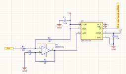
I learned that the incoming signal also has negative zone(max 200mV). And, this ADC accepts 0V-5V as input signal. I'm thinking of sliding signal to the positive zone, but I don't know how can I do that. I tried adding extra voltage on the opamp, but that breaks the gain ratio. How can I do it?

Here is the schematic. (I'm planning to use internal reference in ADC)
 

Attachments

  • Capture.PNG
    Capture.PNG
    82.2 KB · Views: 128

Hi,

basically you want to lift the amplifier ouput a little bit

My recommendation:
Put a resistor (R1) from ADC_REF to OPAMP_+IN

but for it to work you need another series resistor (R2) at the input (AIN to OPAMP_+IN).

so if you wat to lift the output by 250mV (a bit more than the given 200mV).
With a gain of 10 you need to lift the input by 25mV
so let R2 be 100mV. And I guess REF is 4.0V
then R1 = R2 * 4.0V / 0.025V = 100R x 160 = 16k

Klaus
Hi,

Thank you so much for the detailed answer.

How a connection from ADC_REF can lift the amplifier?

I want to lift the output from the opamp by 2V(2.5V, if it should be more than 2V). With a gain of 10, I think I need to lift the input by 200mV or 250mv?

Yes, the internal Vref is around 4.0V. The analog input signal is max +/- 200mV, after amplifying it will be +/- 2V. So, I need to lift 2V if I'm not wrong. Or, I should use an external 5V(ref) for 0-5V ADC input, and lift 2.5V.
 

Hi,

How a connection from ADC_REF can lift the amplifier?
Basically it´s a resistive voltage divider.

Math:
I´m sure you can do the math on your own. ... just by replacing my values with your values.

Klaus
 

Hi,


Basically it´s a resistive voltage divider.

Math:
I´m sure you can do the math on your own. ... just by replacing my values with your values.

Klaus
Thank you again!

I understand, I thought that there was another thing related to reference. I changed V(ref) to 5V, and made math on it for lifting 2.5V (250mv input to opamp).

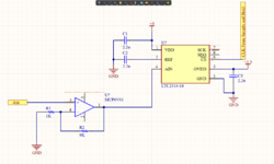
Also, I want to ask about opamp(MCP6V61). The input signal is 1Mhz, so I searched 1 Mhz Gain Bandwidth Products on the mouser site as a filter and chose the smallest Input Offset Voltage. Is there a mistake I made in the selection? Since the signal is at a high frequency and mV level, I'm worried about the opamp being a problem.

If I supply the opamp with 5V(pin 5) and gnd(pin 2), would that be ok?

Best regards
 

Attachments

  • Capture2.PNG
    Capture2.PNG
    49.2 KB · Views: 104

You want the amplifier to reproduce 1 MHz samples without crosstalk of previous samples. Also consider the relation between OP GBW and BW at the actual gain of 10. An OP fitting your requirements will have at least 50 MHz GBW, possibly more.
--- Updated ---

Other than stated in post #1, LTC2314 has no dedicated conversion start input. Synchronous sampling has to be achieved by starting the SPI transmission repeatedly with correct time relation to the 1 MHz sync signal. You didn't yet mention your data procession solution, but it should be capable of doing so.
 
Last edited:
Status
Not open for further replies.

Part and Inventory Search

Welcome to EDABoard.com

Sponsor

Back
Top