Welcome to our site! EDAboard.com is an international Electronics Discussion Forum focused on EDA software, circuits, schematics, books, theory, papers, asic, pld, 8051, DSP, Network, RF, Analog Design, PCB, Service Manuals... and a whole lot more! To participate you need to register. Registration is free. Click here to register now.
You'll usually want to use the standard 6-layer stackup of your PCB manufacturer. It's two cores and three prepreg layers. There's also a default selection for substrate/prepreg thickness, but it can be modified according to special design requirements. Presumed you don't have any, refer to the (cheapest) default stackup.
You do not choose where the prepegs are. It is the PC B manufacturers production methode which determines where the prepeg layers are in your stackup.
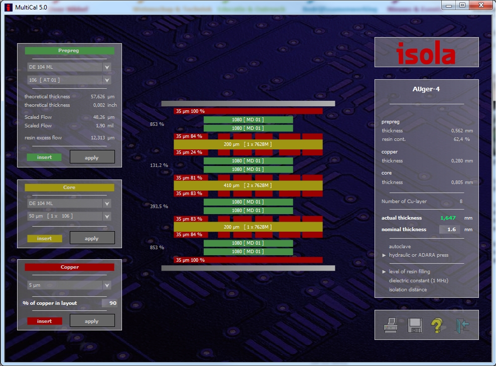
Most PCB manufacturers will use copper foil for the outer layers. With this method you need a prepeg layer to 'glue' the copper foil to a core. You need a prepeg layer between two cores. Have a look at he picture. The green layers are the prepeg layers.
This site uses cookies to help personalise content, tailor your experience and to keep you logged in if you register.
By continuing to use this site, you are consenting to our use of cookies.