Continue to Site

Welcome to EDAboard.com

Welcome to our site! EDAboard.com is an international Electronics Discussion Forum focused on EDA software, circuits, schematics, books, theory, papers, asic, pld, 8051, DSP, Network, RF, Analog Design, PCB, Service Manuals... and a whole lot more! To participate you need to register. Registration is free. Click here to register now.

How can I understand how is GDS connected to Verilog?

unixdaemon

Newbie level 6
Joined
Feb 11, 2023
Messages
14
Helped
0
Reputation
0
Reaction score
1
Trophy points
1
Activity points
137
I've ran the Fusion Compiler on a simple module:
Code:
module top(a1, a2, z);
        input   [0:0] a1;
        input   [0:0] a2;
        output  [0:0] z;

        assign z = a1 | a2;
endmodule

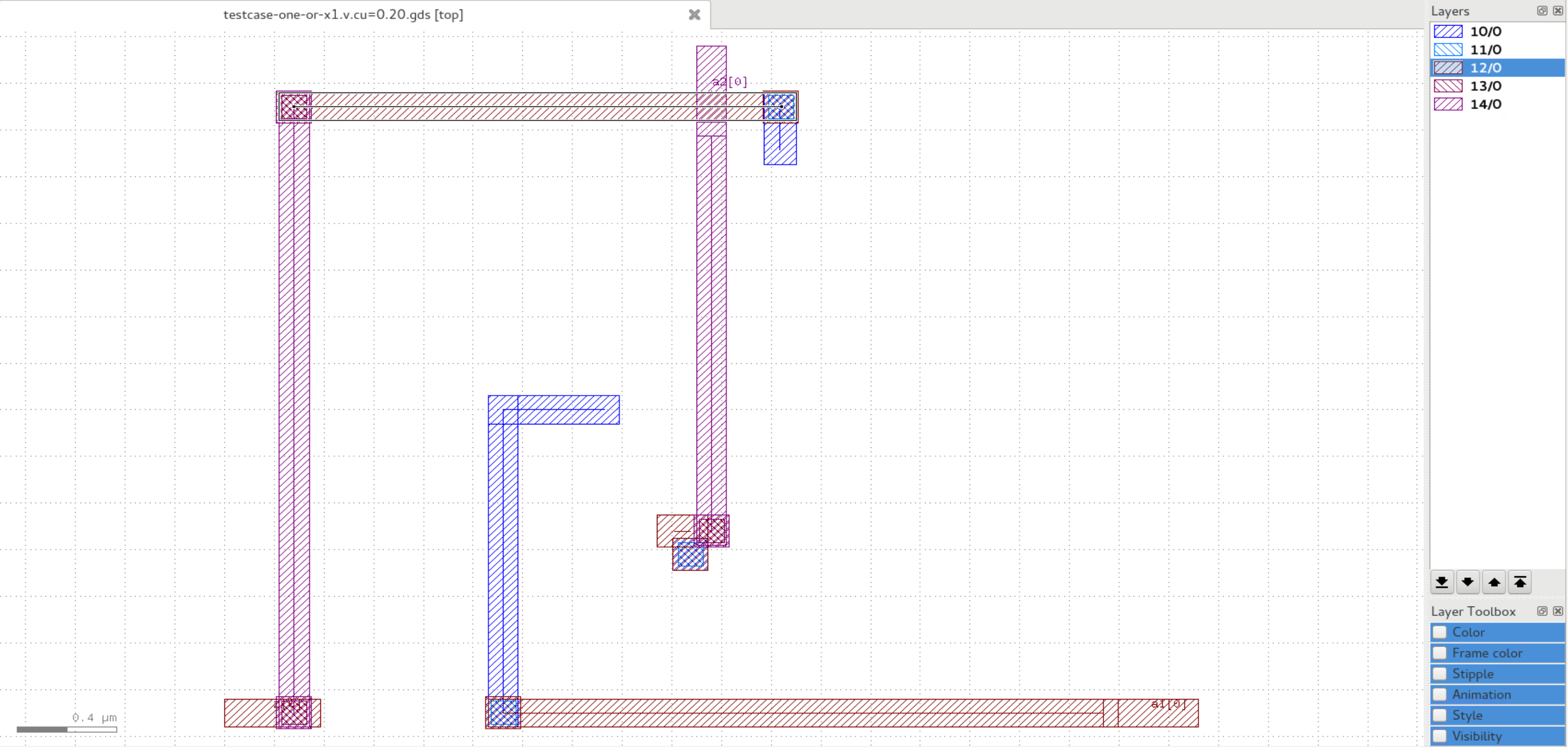
Fusion Compiler generated the GDS file that KLayout shows like this:
1689119983500.png

I have trouble relating the original Verilog code with this GDS image.

How can one understand that there is a single logical-OR gate present here?
Where are the transistors?
Shouldn't the material come close to each other to form NPN or PNP transistors?
And where are VSS and VDD lines? Shouldn't they be always present?
It looks to me that a1[0], a2[0] and z[0] are all disconnected from each other as shown on the above picture.

Larger designs result in more layers in the GDS file.
How to understand what these layers represent since the GDS viewer only shows them as numbers NN/0?

What to read in order to understand the ASIC's GDS structure better?
 
Last edited:
1. Clarify what the technology is. CMOS? In this case we'd expect FET rather than bipolar transistors.
2. To understand the generated semiconductor structures, show the diffusion masks, not only metal.
3. There should be a transistor level netlist.
 
Couple of things here.

Simplest, be sure you are asking klayout for "full hierarchy", cell content
may just not be displaying by default. I think this is under the Display
menu branch but I'm away from the "real" PC.

Next you can look at the "Cells" tab around all the layers stuff, and
expand the hierarchy on the list; under the top level you may see a
couple of objects which turn out to be FETs (if all was set up right).
You can "show as new top" by right-click on any point in the tree if
you want to inspect.

Third, that module to me only informs a logical construct. I see no
"mapping" to a family of logic functions, from there to named gates
and sub-versions (drive strength etc.). But you'd expect a harder fail
(or not?) with a break in the "mapping chain"? Maybe you got one
and just didn't read the details of complaints.
 
> looks like the the gds is generated incorrectly, the cells are not present. only the wires

Yes, I agree.

How can I understand why cells are not present?
I only defined one cell. Other cells must be standard cells.

What steps can I take to understand why the produced GDS file is invalid?
 
Look at my earlier post. What did you tell "Fusion"
about where to find the cells and their route-to
information?

I wonder whether the layout you show, has other
generated views above and below. That it routed at all
indicates some "targets". But perhaps those come from
a different place than the transistor / cell layouts (which
pre-exist).

Presumably there should be a log file from the synthesis
action. What does it hold, for warnings or simple list of
actions performed?

The veriloga is not "structural" (built of transistors and gate
instances). How does the simple logic get mapped to an
(whatever is "|"?) AND gate, or whatever? Why is the verilog
not something like z=and21(a1,a2) - and what would happen
if you -did- attempt a structural verilog instead?
 
"and21" isn't a valid cell name.

I think that the problem is that fusion compiler creates the GDSII file with only wires, and no transistors. The last instruction before "write_gds" is "route_auto".

I think that FC functions fine, it places all wires.
But transistors are added by some other command, which is missing and I just don't know what that command is.

"tsmc18u_slow.tf" is used as a tech file.
Reference cells are taken from the project called "ti_pmc".

(It's amazing that Synopsys doesn't provide a "Getting Started" guide where they should show simple examples of how to use FC using basic testcases. I wonder how do people even learn how to use FC or how do they find answers to questions like this. Their other products, for ex. VC Formal and TCAD, do have detailed getting started guildes, just not FC. I learned VC Formal and TCAD using their getting started guides.)
 
you typically point to another gds file, one that contains the layout of the standard cells, before you do write_gds command. check your documentation.
 

LaTeX Commands Quick-Menu:

Part and Inventory Search

Welcome to EDABoard.com

Sponsor

Back
Top