Continue to Site

Welcome to EDAboard.com

Welcome to our site! EDAboard.com is an international Electronics Discussion Forum focused on EDA software, circuits, schematics, books, theory, papers, asic, pld, 8051, DSP, Network, RF, Analog Design, PCB, Service Manuals... and a whole lot more! To participate you need to register. Registration is free. Click here to register now.

HELP NEEDED IN CPW FED PATCH ANTENNA

Status
Not open for further replies.

saqaw

Junior Member level 3
Joined
Oct 2, 2006
Messages
31
Helped
0
Reputation
0
Reaction score
0
Trophy points
1,286
Activity points
1,536
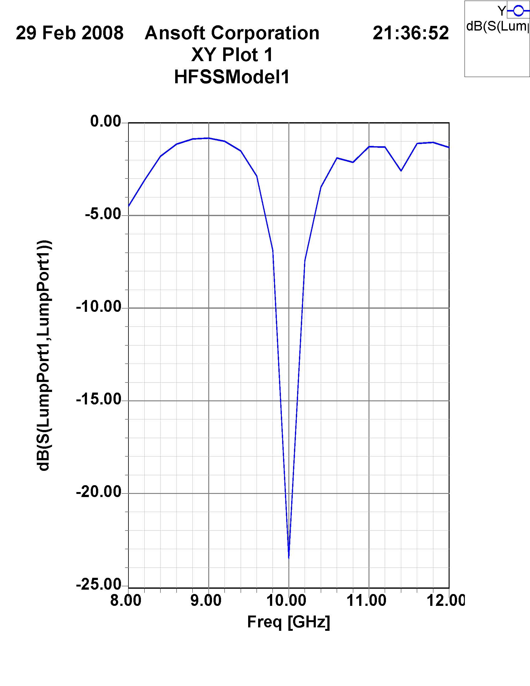
Pl. can anyone indicate that is my design ok or not...I feel that there is problem in assigning the waveport.Although I have designed the waveport according to the rules 4*h and 3*(2g+w).
but i am not getting the results right.


Pl also tell me that if my design for cpw feed line is correct or not...This all is related to my Final year project so I need urgent help ...I am attaching my file...
 

I am waiting for a positive response ............I know there are a lot of experts out there!!!
 

Hi Saqaw,

the integration line you use for your lumped port is definitely wrong. Moreover, your waveport (sheet) should start from z=-2 or so to get the CPW structure in the middle (airbox z_min=-2 in that case). I simulated the new setup and it is fine I guess. Take a look at this figures. since I simulated in HFSS 10.1, I didn't upload it (you cannot open it in previous versions). If you want it, please let me know.

P.S. Take a look at this post: to setup the CPW port.
 

THANKS a lot shameemkabir,

If u can send me the HFSS 10.0 file ,I can have a better look. Dont worry I have got HFSS 10 installed also.

By the way I also moved the waveport a little down. but I didnt chnge the integration line and I amgetting quite good results. I amattaching the file for u to check this..


I didn't have enough time to take a look closely at your design. However, it seems like your port is working fine.

Better still, if you use different integration line what I told you earlier.

Regards,
Shameem
 

Sorry to disturb u again but I have some confusion,

In the tutorials it is written that the wave port size should not exceed lambda/2 in any dimension but also its width should not be less than 3(2g+w).

In my case I have lambda=25mm
g=0.23mm
w=8mm , all these for Zo=50 ohms.

Now my waveport width comes out to be 25.38mm,
but lambda/2=12.5mm.


So what shoould i do now!!!!!!! Any ideas!!!!!!

Even though I am getting good results(with wrong integration line) as shown above, but is it practically possible.
 

Hi Saqaw,

there is no restriction about the maximum size of the port width in general. However, if your cpw mode distribution is not expected you have to play around with the width (changing the width). For your case, please take a look at the port mode distribution whether it is expected or not.

what about the value of w, g? were these already given for your design or you arbitrarily select these? In my view w=8 mm is really high.

best regards,
Shameem
 

hi i am designing a cpw feed patch antenna and have a question my cpw feed network is embedded between two substrated and the patch is on the top of upper substrate can you please tell me the design rules for values of g and w and what should be the lenght of the cpw line.

Added after 1 minutes:

oh forgot to mention what are the limits on values of g wnd w with respect to substarte height

Added after 8 minutes:

can you please check where i am going wrong
 

Status
Not open for further replies.

Part and Inventory Search

Welcome to EDABoard.com

Sponsor

Back
Top