walker5678
Full Member level 3
Is this method OK?
Hi,
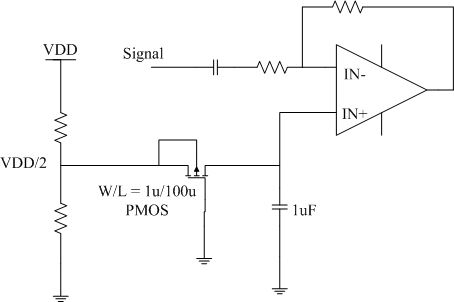
Attached file is an amplifier diagram, in which the IN+ bias voltage is generated by the resistor devider. When there is supply voltage variation, the IN+ will variate, and thus make PSRR bad.
I think about a method to add a W/L=1u/100u PMOS as a large resistor between the 1uF bypass capacitor and the VDD/2, so the variation of bypass capacitor voltage will reduced much, and so as to enhance PSRR performance.
Is this method OK?
thanks
Hi,
Attached file is an amplifier diagram, in which the IN+ bias voltage is generated by the resistor devider. When there is supply voltage variation, the IN+ will variate, and thus make PSRR bad.
I think about a method to add a W/L=1u/100u PMOS as a large resistor between the 1uF bypass capacitor and the VDD/2, so the variation of bypass capacitor voltage will reduced much, and so as to enhance PSRR performance.
Is this method OK?
thanks