BackerShu
Member level 3
I want to design an OTA for SH circuit in Pipelined ADC and some of the important specicications are,
Vdd=1.2V
VCMI=VCMO=0.5V
Adc>96dB
GBW>400MHz
SR>300V/us
CL=Cc=5pF(for low-noise)
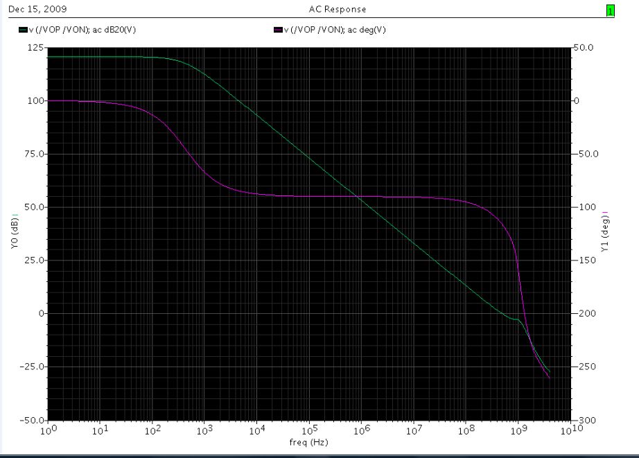
The two stage folded-cascode gain-boosting OTA with hybrid cascode compensation is chosen to meet the spec(the circuit woul be given in Fig6). The AC simulation shows that the DC gain is 115dB, GBW is 500MHz and the PM is 67degree.
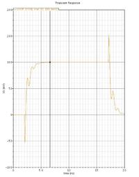
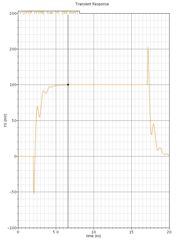
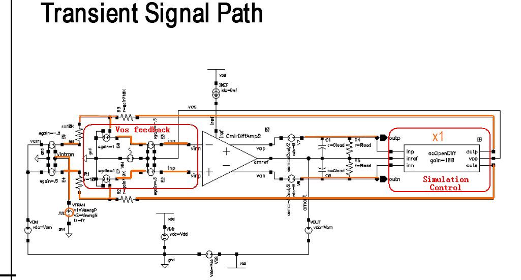
There are something about the settleing beheavior that I can't handle. Fig1~Fig4 show the settling beheavior of the OTA and Fig5 is the testbench circuit.
Fig1
 [/
[/
Fig2
[url=http://obrazki.elektroda.pl/97_1260714761.jpg] [/
[/
Fig 3
[url=http://obrazki.elektroda.pl/37_1260714837.jpg]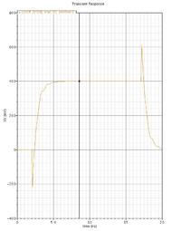 [/
[/
Fig 4
[url=http://obrazki.elektroda.pl/57_1260714916.jpg]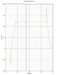 [/
[/
Fig 5
[url=http://obrazki.elektroda.pl/97_1260715213.jpg]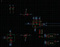 [/
[/
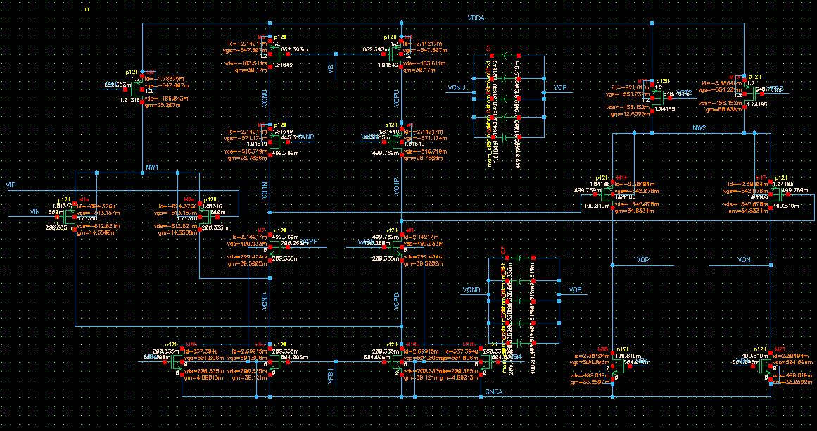
Fig 6 shows the architecture of the OTA(bias and the gain-boosting amp is omitted for simplify) and the node voltage of the DC simulation results.
[url=http://obrazki.elektroda.pl/10_1260715724.jpg]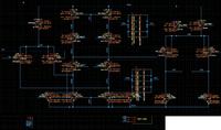 [/
[/
Fig 7 shows the poles/zoles of the main OTA without the gain-boosting amp
[url=http://obrazki.elektroda.pl/12_1260715935.jpg]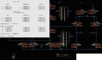 [/
[/
Fig 8 shows the poles/zoles of the main OTA with the gain-boosting amp
[url=http://obrazki.elektroda.pl/4_1260716026.jpg]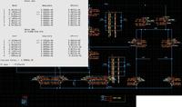 [/
[/
these are all the pre-simulation results and I'm not sure if the settling behavior is right or if it will works when applied in Pipelined ADC. Can someone helps me to explain the settling behavior and give me some tips on how to arrange the complex poles/zoles for fast settling.
Also any comment would be appreciated.
Vdd=1.2V
VCMI=VCMO=0.5V
Adc>96dB
GBW>400MHz
SR>300V/us
CL=Cc=5pF(for low-noise)
The two stage folded-cascode gain-boosting OTA with hybrid cascode compensation is chosen to meet the spec(the circuit woul be given in Fig6). The AC simulation shows that the DC gain is 115dB, GBW is 500MHz and the PM is 67degree.
There are something about the settleing beheavior that I can't handle. Fig1~Fig4 show the settling beheavior of the OTA and Fig5 is the testbench circuit.
Fig1
 [/
[/Fig2
[url=http://obrazki.elektroda.pl/97_1260714761.jpg]
[/Fig 3
[url=http://obrazki.elektroda.pl/37_1260714837.jpg]
[/Fig 4
[url=http://obrazki.elektroda.pl/57_1260714916.jpg]
[/Fig 5
[url=http://obrazki.elektroda.pl/97_1260715213.jpg]
[/Fig 6 shows the architecture of the OTA(bias and the gain-boosting amp is omitted for simplify) and the node voltage of the DC simulation results.
[url=http://obrazki.elektroda.pl/10_1260715724.jpg]
[/Fig 7 shows the poles/zoles of the main OTA without the gain-boosting amp
[url=http://obrazki.elektroda.pl/12_1260715935.jpg]
[/Fig 8 shows the poles/zoles of the main OTA with the gain-boosting amp
[url=http://obrazki.elektroda.pl/4_1260716026.jpg]
[/these are all the pre-simulation results and I'm not sure if the settling behavior is right or if it will works when applied in Pipelined ADC. Can someone helps me to explain the settling behavior and give me some tips on how to arrange the complex poles/zoles for fast settling.
Also any comment would be appreciated.
 [/
[/ [/
[/ [/
[/