Continue to Site

Welcome to EDAboard.com

Welcome to our site! EDAboard.com is an international Electronics Discussion Forum focused on EDA software, circuits, schematics, books, theory, papers, asic, pld, 8051, DSP, Network, RF, Analog Design, PCB, Service Manuals... and a whole lot more! To participate you need to register. Registration is free. Click here to register now.

Fully differential OTA design for low power SC integrator

Status
Not open for further replies.

Fabien

Full Member level 1
Full Member level 1
Joined
May 22, 2011
Messages
96
Helped
10
Reputation
20
Reaction score
10
Trophy points
1,288
Location
Grenoble
Visit site
Activity points
2,025
Good morning everyone,

I'd'like to design a simple fully differential OTA for a switched capacitor integrator. As it needs to be very low power, I'm wondering how to start the design and how to fixe the W and L of the transistors? The design I made doen't have the common mode in the middle range (Vdd/2).
I read some papers about the Gm/ID methodology, but as the best case is in moderate inversion, I'm wondering how to achieve this requirements. What is a typical procedure to design an OpAmp?

Can anyone help me how to start a design?

Thank you
 

strong inversion, moderate inversion, weak inversion all depends on what you're power specs are and what linear range, noise etc you want. Any specs?
 

Don't need to be linear.
Low frequency (the switched capacitors are 32kHz cloked), just need to be low power. Low power doesn't need anything, but if I can have 1µA instead of 10µA it's better!
 

I'd'like to design a simple fully differential OTA for a switched capacitor integrator. As it needs to be very low power, I'm wondering how to start the design and how to fixe the W and L of the transistors? The design I made doen't have the common mode in the middle range (Vdd/2).

I read some papers about the Gm/ID methodology, but as the best case is in moderate inversion, I'm wondering how to achieve this requirements. What is a typical procedure to design an OpAmp?

Can anyone help me how to start a design?

Here's a low power rail-to-rail-input and -output OpAmp with a current consumption < ½µA, which I designed several years ago for a 0.18µm process. Nearly all its MOSFETs are operating in weak inversion mode. Hope this helps.
low_power_rail_to_rail_opAmp_schematic.gif
 

Thank you very much Erikl for your help!
Actually, I'm looking at your post from "06-11-09, 17:19" regarding to the gm/ID methodology. I don't know if it's the best way to start a design, but I'm wondering how could I simulate the VA voltage? I've the gm/Id vs Vgs curve (dId/dVgs/Id) ) and the ro curve (dVds/dId) but for the early voltage, I only can compute it by hand calculation.
Any idea how to have this data and if it's a good way to start?

Thank you
 

... regarding to the gm/ID methodology. I don't know if it's the best way to start a design
Sure, it's a very good way to start and complete a design, IMHO.

I'm wondering how could I simulate the VA voltage? I've the gm/Id vs Vgs curve (dId/dVgs/Id) ) and the ro curve (dVds/dId) but for the early voltage, I only can compute it by hand calculation. Any idea how to have this data and if it's a good way to start?

See this thread!
 
  • Like
Reactions: Fabien

    Fabien

    Points: 2
    Helpful Answer Positive Rating
I got the VA vs Vds curve from your thread! I calculated it by hand and I got the same results!
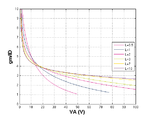
But, is there a way to plot gm/ID vs VA ? Here is my plot.

thanks
 

Attachments

  • Gm-ID VA.png
    Gm-ID VA.png
    20.4 KB · Views: 138


erikl,

"Here's a low power rail-to-rail-input and -output OpAmp with a current consumption < ½µA, which I designed several years ago for a 0.18µm process. Nearly all its MOSFETs are operating in weak inversion mode. Hope this helps."

I have a feeling this circuit will have an ill-defined quiescent current in its output stage. At balance and driving no load, the first stage amplifier should have an output voltage of Vgs commensurate with the second stage's Q-current equaling the first stage's. The NMOS and PMOS input stages will have different offset voltages, and since they are forced to have equal input voltages it will manifest as an output voltage offset (since their currents aren't summed but are instead independently converted to voltage); rather than Vgs, each output will be Vgs±Voffset*gm*ro (plugging in appropriately adjusted values for Voffset and ro). Depending on the offset magnitude and the value of ro, this could cause some serious quiescent current variations (i.e., the output stage's Q-current could be zero, or it could be tens of µA) and possibly prevent operation altogether.

Not to mention, it doesn't appear like it should work well with rail-to-rail inputs.

I would think this should show up in Monte Carlo sims. Has this circuit been built in silicon?
 
  • Like
Reactions: erikl

    erikl

    Points: 2
    Helpful Answer Positive Rating
Hello ZekeR, very well retraced ;-)

I have a feeling this circuit will have an ill-defined quiescent current in its output stage. At balance and driving no load, the first stage amplifier should have an output voltage of Vgs commensurate with the second stage's Q-current equaling the first stage's. The NMOS and PMOS input stages will have different offset voltages, and since they are forced to have equal input voltages it will manifest as an output voltage offset (since their currents aren't summed but are instead independently converted to voltage); rather than Vgs, each output will be Vgs±Voffset*gm*ro (plugging in appropriately adjusted values for Voffset and ro).
You are quite right, but we used it only as buffer (for reference voltages).

Depending on the offset magnitude and the value of ro, this could cause some serious quiescent current variations (i.e., the output stage's Q-current could be zero, or it could be tens of µA) and possibly prevent operation altogether.

I would think this should show up in Monte Carlo sims. Has this circuit been built in silicon?
Right again! MC sims showed huge output stage current variations: opr2r_monteCarlo_outputStageCurrent.png
So we spent it a folded mesh minimum selector /1/ class AB quiescent output current control circuit folded_mesh_min_selector.gif ... before going to silicon.

/1/ Klaas-Jan de Langen, Johan H. Huijsing: "Compact Low-Voltage Power-Efficient Operational Amplifier Cells for VLSI"
IEEE JSSC Vol. 33 No. 10, Oct-1998

Not to mention, it doesn't appear like it should work well with rail-to-rail inputs.
Not really, but good enough for our purposes: opr2r_DC_response.gif It worked well for input voltages Vthn ≦ Vinp ≦ VDD-|Vthp| . VDD was 2.5V±10% .

BTW: the shown circuit wasn't thought of being rebuilt (anyway the OP wanted a fully differential amplifier); it was just thought to show an example for a low power amplifier working in subthreshold mode.
 
  • Like
Reactions: ZekeR

    ZekeR

    Points: 2
    Helpful Answer Positive Rating
It should be possible with the help of ADE's calculator tool. See the last sentence in my posting!

It should be possible with the help of ADE's calculator tool. See the last sentence in my posting!

So... I used the ADE calculator to find gm over ID and VA. Then I used Matlab to plot gm/ID versus VA for different L values. Here is the plot:

Here are my questions:

Do these curves look good or not? Just wondering if I made a calculation mistake.
For high L, we can have a high bandwidth. And the higher gm/ID, the best efficiency. So if I understand, the best thing is to use a huge gm/Id, but in this case VA will be small and the ro. What is the strategy to adopt once we got these curves?

I think these curves depend on the technology. So why is there no kind of charts? Yes, for sure when we now the methodology it could be quite easy and quicly to get the curves!

thanks
 

Attachments

  • gmoverID_VS_VA.png
    gmoverID_VS_VA.png
    9.3 KB · Views: 120

Do these curves look good or not? Just wondering if I made a calculation mistake.
They look reasonable. And they match with your above gm/Id and VA vs. sweep-time curves.

For high L, we can have a high bandwidth.
Not necessarily: For high bandwidth you just need large gm, for which you need high Id values. And this is better achieved (means: area and parasitic cap saving) by large gm/Id causing low VA values. Actually high frequency amplifiers tend to use small transistor lengths.

And the higher gm/ID, the best efficiency. So if I understand, the best thing is to use a huge gm/Id, but in this case VA will be small and the ro. What is the strategy to adopt once we got these curves?
Depends on quite a lot of your priority requirements: high UGF vs. low power, transistor matching (offset) vs. area consumption, (low) noise ...

For large DC gain - which is proportional to (gm/Id)*VA - your curves show a clear tendency for large VA ≙ small gm/Id values - good for high gain/low frequency amplifiers.

BTW: your curves show a practically length-independent (apart from L=0.5) cross-point @ gm/Id=4 and VA≈17V.
Seems a nice compromise for starting a design calculation with all equal transistor lengths (e.g. 1µm) , scaling necessary fT's by using different Id's (via a single Ibias).
 

Thank you, it seems to be clear.

I do not care about the area consumption, priority is low power, the GBW could be tens of kHz (Switched capacitors at 32kHz) and a gain of 100 could be good enough. But, the CMRR must be low (as low as possible, so maching is important).
This curves have been simulated with W=2µm.
So for starting, you suggest to design a simple differential amplifier and current mirror for biasing and test with different Ids?
 

I do not care about the area consumption, priority is low power, the GBW could be tens of kHz (Switched capacitors at 32kHz) and a gain of 100 could be good enough.

... the CMRR must be low (as low as possible, so maching is important).

A gain of 100 is quite a lot for a single stage OTA (single stage: because you want to save power), but can surely be achieved for such a low-frequency amplifier. Because you can operate in subthreshold (weak inversion) mode, use a large VA - medium gm/Id combination with a relatively long L - I'd use L≧3µm - as you don't have area consumption problems. For the input transistors, I'd use L=10µm - this is good for your CMRR requirement.

This curves have been simulated with W=2µm.
So for starting, you suggest to design a simple differential amplifier and current mirror for biasing and test with different Ids?

What is your process size? VDD? Your technology current? I guess you could get along with currents of the order of several 100nA.
 
  • Like
Reactions: Fabien

    Fabien

    Points: 2
    Helpful Answer Positive Rating
I tried but... still blocked!
My process is 90nm, Vdd 3V (should work from 2.4 to 3V: batteries requirements). You said from "thread162125: you can choose a convenient L-VA combination, e.g. 0.6µm - 10.2V for M3-M4" but what about the W? Some papers suggest to plot gm/ID vs ID/W/L, what's the difference btw gm/ID vs VA?

I think the design depends on the offset at the inputs. Of course, we can't have a few mV at the gates of the inputs transistors, and does the gain or the overall performances depends on the inputs voltages?

I still didn't understand how to size the transistors :(
danke schön
 

... but what about the W? Some papers suggest to plot gm/ID vs ID/W/L
Sure: from this curve you get the W/L ratios.

what's the difference btw gm/ID vs VA?
Via the necessary DC gain you get VA and then an upper limit for the gm/Id value from this curve, considering L

I think the design depends on the offset at the inputs. Of course, we can't have a few mV at the gates of the inputs transistors
So use a large enough L for the input transistors (in order to get a good layout matching, you could interdigitate them, or split them into an array).

... and does the gain or the overall performances depends on the inputs voltages?
It shouldn't, as you probably will have a large feedback ratio (Av[open loop] / Av[closed loop]).

I still didn't understand how to size the transistors :(
Now what else do you need?

- First decide on your Id current, considering your low frequency and low power requirements, for starting I'd recommend 100nA per (vertical) current branch (which you'll need 4..5 times in total). Design your bias supply so that you need to change only one single supply current for acting on all branches. This facilitates later changes.

- You have your gm/Id (decide on a highest possible value (considering the necessary Av value via the gm/Id vs. VA curve), to operate in weak inversion mode because you want low power consumption, and because you seem to have no area limit, and because you need no high frequency transistors.)

- From the Id/(W/L) vs. gm/Id curves (different for NMOS & PMOS) you get the W/L values for all your transistors. For such low currents in a 90nm process, it's quite possible to get W/L < 1 values. Hope your sim. models support this! If not, try larger Id values (or larger gm/Id values - but this will result in lower DC gain because of lower VA).

- You have already decided on L (at least on an L range) when you considered your gm/Id vs. VA curves. If you can get enough DC gain with VA≈17V and gm/Id≈4V-1 (your curves' cross-point), you can live with a min. L of 1µm (which is already a factor of 11 larger than your process Lmin), otherwise (for larger VA and lower gm/Id values) I'd recommend L=3..5 , larger L values don't achieve much better gm/Id values. For the current mirror transistors I'd recommend to use an L value a factor of 2 larger, for more mirror accuracy. In order to get a low offset voltage I'd suggest to use L=10µm (because you don't have an area consumption problem) for the input transistors.

- Now with having decided on all the transistors' L values, you can calculate their widths from the 2 values which you got from the 2 Id/(W/L) vs. gm/Id curves (for NMOS & PMOS).

- Then analyze and optimize by simulations.
 
  • Like
Reactions: Fabien

    Fabien

    Points: 2
    Helpful Answer Positive Rating
Thank you very much for your help, it's really much more clear from now.
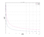
I simulated the gm/ID vs ID/W/L and I got this plot. So, the thing is that in weak inversion (gm/ID = 4) ID/W/L = 3.6 and 13.7 for PMOS and NMOS respectively. With a 100nA current, L/W = 137 (Nmos) If I choose L=10µm for the input, I should choose W= 1370µm! It's impossible for the simulator! Are these plots wrong? Or may be I should choose a different gm/ID value, in moderate or strong inversion?
 

Attachments

  • gmID_vs_IDWL_NP.png
    gmID_vs_IDWL_NP.png
    14.8 KB · Views: 144

Are these plots wrong?
No, I don't think they are wrong, even if I had estimated a factor of 10 lower for the Id/(W/L) value (i.e. x 10-6 at the end of the abscissa) for the 90nm process. Pls. check once more!

However, I think your calculation method is wrong. Let's take the NMOS example with the Id/(W/L) value from your curve:
gm/Id=4 --> Id/(W/L) = 13.7µA ; W/L = Id/13.7µA = 0.1µA/13.7µA = 0.0073 ; L=10µm --> W=0.0073*L = 0.073µm = 73nm , which is below your min. permissible width. So you would need even a longer length than 10µm.

Or may be I should choose a different gm/ID value, in moderate or strong inversion?
Now, the other way round: you should choose a larger gm/ID value, more in weak inversion, which gives you even better transconductance (gm) efficiency, but will decrease your DC gain because of lower VA (and your UGB).

BTW: I'd recommend to study D. Binkley's book "Tradeoffs and Optimization in Analog CMOS Design", which explains the operation and W/L calculation in different inversion modes in terms of the process-dependent technology current and the Inversion Coefficient (IC), which is more simple to be understood, IMHO.
 
Last edited:
  • Like
Reactions: Fabien

    Fabien

    Points: 2
    Helpful Answer Positive Rating
OK, I think I understood most of the things except some points:
you said : "choose a larger gm/ID value, more in weak inversion, which gives you even better transconductance (gm) efficiency, but will decrease your DC gain because of lower VA (and your UGB)"

The gain Av = gm x ro = gm x VA/ID, so with a high gm/ID, the gain decrease, I think it's interressant to work with small gm/ID because of huge VA! So what is the real need to work in weak inversion if we have a little gain?

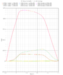
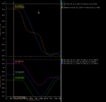
Other point, I ran a lot of simulation but a current of 100nA, with the chart I have I can't get a big gm/ID because of a small ID/W/L (the possible values for W and L are between 0.4 and 10µm) but I got a gain of 60dB in the first differential pair (inputs are -6dB)! Unfortunately I can't get this at the output stage! What is weard is that I'm not able to find it with calculation! Both transistors seems to be in weak inversion because ID/W/L = 0.2µ for the PMOS (current mirror) and = 2.5µ for the NMOS. So I'm not able to understand why the gain is so important!
Here is the simple schematic with the results;

If I change the input offsets, the gain change also. The current simulation is with a 1Vdc offset, if not, I'm loosing a lots of dBs!

May be this design will not working but if I understand the concept I need a higher biasing current because of the best W/L I can get is 0.04 so in order to have a reasonnable VA I need 20µ so ID= 0.8µA at least.
Am'I right?
 

Attachments

  • simu_rlts.png
    simu_rlts.png
    16.3 KB · Views: 110
  • OTA_miller.png
    OTA_miller.png
    37 KB · Views: 96

Status
Not open for further replies.

Part and Inventory Search

Welcome to EDABoard.com

Sponsor

Back
Top