Continue to Site

Welcome to EDAboard.com

Welcome to our site! EDAboard.com is an international Electronics Discussion Forum focused on EDA software, circuits, schematics, books, theory, papers, asic, pld, 8051, DSP, Network, RF, Analog Design, PCB, Service Manuals... and a whole lot more! To participate you need to register. Registration is free. Click here to register now.

Getting the VA (or VE) Early voltage for a NMOS and a PMOS transistor in CADENCE?

Status
Not open for further replies.

AMSA84

Advanced Member level 2
Joined
Aug 24, 2010
Messages
577
Helped
8
Reputation
16
Reaction score
8
Trophy points
1,298
Location
Iberian Peninsula
Activity points
6,178
Hi guys,

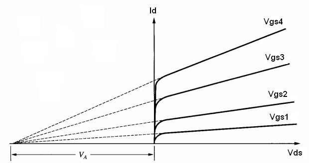
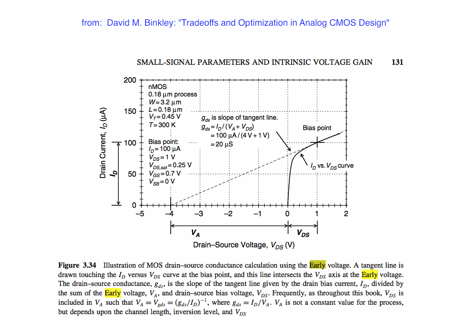
I want to get the early voltage for the PMOS and NMOS transistor. I know that I have to get the slope of the Id vs Vds curves, but I don't know how to do it.

Can someone help me out here? I am using AMS DK 0.35um.

Kind regards.
 

In saturation mode the Early Voltage VA practically doesn't depend on the operation point, s. here:

How to calculate VA you can see from this figure:

Hence VA = (ID/gds) - VDS

You can calculate it manually, or have it calculated by ADE's calculator.
 
Hi erik,

I see. What I am thinking to do is the DC sweep from 0V up to 3.3V of an NMOS transistor with Vgs = 1V. Then, get two points from the characteristic curve Ids vs Vds and then calculate the VA through the equation of the line (y =mx + b).

Now that you showed that figure, one can compute the VA using that equation. Is that as accurate than the y=mx+b approach?

All the values in VA = (Id/gds) - Vds are taken from the DC analysis? (DC operation points)

By the way, that gds is the value that we can use to determine r_o? r_o = 1 /gds? On my DC analysis I got 792.8nS. Is that normal? My W/L was 10/10.

The DC analysis result:
untitled.PNG

EDIT: I tried to simulate the circuit and I got this curve: (it's a strange result, do you know what can be wrong?)
snapshot1_edited.PNG

I used 10/10, swept from 0 up to 2.5V (Vds) with vgs = 1.

If I compute with the values that I got from the DC analysis, as you can see in the 1st image, I get a VA of ~309V. There is something wrong here, right?

Kind regards.
 

What I am thinking to do is the DC sweep from 0V up to 3.3V of an NMOS transistor with Vgs = 1V.
Right so!

Then, get two points from the characteristic curve Ids vs Vds and then calculate the VA through the equation of the line (y =mx + b).
Now that you showed that figure, one can compute the VA using that equation. Is that as accurate than the y=mx+b approach?
Actually it's identical.

All the values in VA = (Id/gds) - Vds are taken from the DC analysis? (DC operation points)
Also in DC analysis, gds is computed as inclination of the curve: gds = δId/δVds . Compare it to the value of Id/Vds !

By the way, that gds is the value that we can use to determine r_o? r_o = 1 /gds? On my DC analysis I got 792.8nS. Is that normal? My W/L was 10/10.
Yes, that's the correct value for r_o (≈ 1.25MΩ), if you consider the transistor alone, i.e. isolated from any other circuit elements, exactly as shown in your test schematic.

I tried to simulate the circuit and I got this curve: (it's a strange result, do you know what can be wrong?) I used 10/10, swept from 0 up to 2.5V (Vds) with vgs = 1.
It's really weird; I can't understand the buckle @ Vds=2.2V .

If I compute with the values that I got from the DC analysis, as you can see in the 1st image, I get a VA of ~309V.
Correct!

There is something wrong here, right?
gds measured between (say) Vds=1.7..1.9V could result in a similar value, I'd guess. Computed with Vds values between (say) 2.2..3.0V , a much lower VA value would result, of course.
 

gds measured between (say) Vds=1.7..1.9V could result in a similar value, I'd guess. Computed with Vds values between (say) 2.2..3.0V , a much lower VA value would result, of course.

So what you are telling me is that the value of gds is being taken in the interval of 1.7V to 1.9V? Why he computes the value of gds around that interval? What is the criteria?

I didn't understood your point in the quote. Could you develop a little more?
 

So what you are telling me is that the value of gds is being taken in the interval of 1.7V to 1.9V? Why he computes the value of gds around that interval? What is the criteria?
No: the gds value had been computed exactly at the DC operation point shown in your 1st image above : @ vds=vgs=2.5V

I didn't understood your point in the quote. Could you develop a little more?
Which quote? Could you explain a little more?
 

You are right about the vgs, I didn't notice that. I posted the wrong image. The right image is this one here:

VEDADEIRO2.png

About the quote that I was referring to is this one:

gds measured between (say) Vds=1.7..1.9V could result in a similar value, I'd guess. Computed with Vds values between (say) 2.2..3.0V , a much lower VA value would result, of course.

However, I have that the calculation with that Ids vs Vds curve using the y = mx + b and it gave me 16.5V. Using the approach that you posted in your first post it gives me around 180V. Can you explain why?
 

However, I have that the calculation with that Ids vs Vds curve using the y = mx + b and it gave me 16.5V. Using the approach that you posted in your first post it gives me around 180V. Can you explain why?

Not really, because this should be identical, as I said above:
y=mx+b -> Id=(δy/δx)*(Vds+VA) = gds*(Vds+VA) = gds*Vds+gds*VA -> VA = (Id-gds*Vds)/gds = Id/gds - Vds
 

Status
Not open for further replies.

Part and Inventory Search

Welcome to EDABoard.com

Sponsor

Back
Top