This would be correct if you could trust your gm/Id vs. VA curves. But see below:you said : "choose a larger gm/ID value, more in weak inversion, which gives you even better transconductance (gm) efficiency, but will decrease your DC gain because of lower VA (and your UGB)"
Thinking twice, I reviewed Binkley's curves on these contexts, and they seem quite different from yours:The gain Av = gm x ro = gm x VA/ID, so with a high gm/ID, the gain decrease, I think it's interressant to work with small gm/ID because of huge VA! So what is the real need to work in weak inversion if we have a little gain?
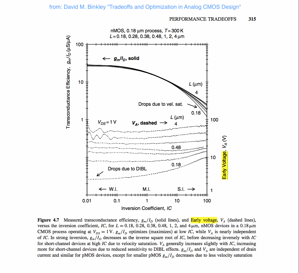
VA doesn't drop so much with increasing gm/Id as in your figure. It's from a 180nm process, but anyway ...
Other point, I ran a lot of simulation but a current of 100nA, with the chart I have I can't get a big gm/ID because of a small ID/W/L (the possible values for W and L are between 0.4 and 10µm) but I got a gain of 60dB in the first differential pair (inputs are -6dB)! Unfortunately I can't get this at the output stage! What is weard is that I'm not able to find it with calculation! Both transistors seems to be in weak inversion because ID/W/L = 0.2µ for the PMOS (current mirror) and = 2.5µ for the NMOS. So I'm not able to understand why the gain is so important! Here is the simple schematic with the results
I think your simulation schematic isn't ok:
1. I don't see if your stimuli sources V3 & V4 include any DC voltages. If they don't, you have DC=0V at both inputs. Also, see the *Error* messages at M10 & M12. Check your operation point voltages!
2. Both ac sources seem to stimulate common mode ac voltages. So how could you expect much gain at all?
You need full DC feedback from Vout+ to Vin- and from Vout- to Vin+ (e.g. using 1GΩ feedback resistors plus 1GF caps to GND), inserting a single unit ac source between one of the feedback points and one of the Vin inputs. Cf. my schematic below. Or use SPECTRE's iprobe method.
Of course: your sim schematic doesn't use full DC feedback! So it simply moves away from a (perhaps previously) good operation point.If I change the input offsets, the gain change also. The current simulation is with a 1Vdc offset, if not, I'm loosing a lots of dBs!
May be this design will not working but if I understand the concept I need a higher biasing current because of the best W/L I can get is 0.04 so in order to have a reasonnable VA I need 20µ so ID= 0.8µA at least.
Am'I right?
Not necessarily. I tried a similar design (single ended only) in weak inversion mode, using W/L=8 for nMOS and W/L=20 for pMOS. Got nearly 60dB DC gain and a UGB≈350kHz with bias currents of 100nA and Cload=100fF. Unfortunately I've got no access to Cādence tools nor to a 90nm lib, but I think my transistors' properties should be close to theirs. See the PDF below!
I forgot to mention: In no way this is a complete, optimized circuit! This is a quick shot I made for the most simple type of a 2-stage Miller-OTA, estimated and calculated for a low-power low-frequency circuit operating at the onset of deep weak inversion mode (IC≈0.01 for 90nm process), not at all optimized for power/speed nor equipped with the Miller cap, which is surely necessary for low gain feedback operation. But IMHO it's a good start point for optimizing such a design.
Attachments
Last edited: