KingMoshe
Member level 2
Hi,
When my fpga got 3.3v it take 28mS untill fpga wake up and the internal clock start working.
During this 28mS my output gpio get unvalid value of 0.9v even though the IO pulled down as can see in the picture. Any idea why during wake up the IO is not absolute LOW?
GPIO is defined push pull mode.
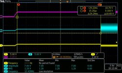
When my fpga got 3.3v it take 28mS untill fpga wake up and the internal clock start working.
During this 28mS my output gpio get unvalid value of 0.9v even though the IO pulled down as can see in the picture. Any idea why during wake up the IO is not absolute LOW?
GPIO is defined push pull mode.