Continue to Site

Welcome to EDAboard.com

Welcome to our site! EDAboard.com is an international Electronics Discussion Forum focused on EDA software, circuits, schematics, books, theory, papers, asic, pld, 8051, DSP, Network, RF, Analog Design, PCB, Service Manuals... and a whole lot more! To participate you need to register. Registration is free. Click here to register now.

PLL implementation through FPGA

sushl

Junior Member level 2
Joined
Aug 22, 2018
Messages
24
Helped
0
Reputation
0
Reaction score
0
Trophy points
1
Activity points
238
Hello All i'm looking to implement a PLL with the following specification through rtl code.

Requirement:
Develop an RTL PLL (phase-locked loop) logic with holdover functionality to ensure continuous phase synchronization of the output signal (pll_out) to the reference signal (signal_1) even during temporary unavailability of signal_1.
Functional Specifications:
  1. Input Signals:
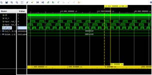
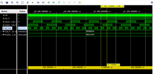
    • signal_1: 8KHz Phase-synced Reference Clock
    • signal_2: 8KHz Local Clock
    • clk_ref: 25MHz Clock
  2. Output Signal:
    • pll_out: Output of PLL locked to signal_1
  3. Normal Operation:
    • When signal_1 is present, pll_out should be phase-locked to signal_1.
  4. Holdover Operation:
    • When signal_1 becomes unavailable, the pll_out should enter holdover mode.
    • In holdover mode, pll_out should maintain the last known phase of signal_1.
    • pll_out should use signal_2 as the 8KHz reference clock to maintain phase synchronization.
  5. Recovery from Holdover:
    • When signal_1 becomes available again, pll_out should smoothly transition out of holdover mode and regain phase synchronization with signal_1.
Non-Functional Specifications:
  1. Performance:
    • The PLL should achieve rapid phase synchronization with the input signals.
    • The PLL should maintain low phase and frequency jitter in both normal and holdover modes.
  2. Resource Utilization:
    • The PLL should minimize resource utilization on the FPGA or ASIC.
  3. Robustness:
    • The PLL should be tolerant to occasional glitches or noise on the input signals.
  4. Testability:
    • The PLL should include design features for easy testing and verification.


      Since PLL's inside my FPGA typically operate at MHz input range i cannot use inbuilt PLL primitives or ip. My device is a cycloneiv fpga.
 
Implement a phase detector to compare the phase difference between signal_1 and pll_out. Commonly used phase detectors include edge counters or D flip-flops.
Divide the 25MHz clock (clk_ref) to generate an 8kHz clock signal that will be used as the clock source for the PLL.
Develop control logic that switches between normal operation and holdover mode based on the availability of signal_1. When signal_1 is available, the PLL should be in normal mode, phase-locked to signal_1. When signal_1 is unavailable, the PLL should switch to holdover mode and use signal_2 as the reference clock.
 
The requirement for fast acquire and the one to "indefinitely" ride
out ref clk loss seems "dissonant".

I could suggest that you want some modality there. Like (say) a
loop filter that is very fast, unlocked but very slow, once locked;
also a "activity detect" on the ref clk (and maybe feedback too)
which will disable the charge pump (or its digital accumulator
equivalent) so that "last correct" state is held. Probably ought to
throw a flag though, just so somebody above, knows.

If it's all-digital then holding the freq should be pretty easy,
but getting to the actual holding can only happen once the
"no tone" decision is made, which would be maybe 10 cycles
for a variable frequency range, fewer if it's "8kHz or nothing,
in a heartbeat". But making things not flake out from lesser
spurii wants some idea of what those might be, short of total
and permanent / long term clock loss.

Yes which is why i need to modify the logic to start and phase align the standalone clock signal_2 with the signal_1 and pass it out through pll.

Been looking up loop filter, vco counter approach and tried to implement it through code.
here is my implementation.
Code:
module phase_detection_correction_vd

  (
        rst_n,
        ref_clk,         //High Freq. Ref. Clock using which a low Freq. to be measured
        input_signal_1,  // Input signal 1, Holdover functionality to be implemented for loss of this signal
        input_signal_2,  // Input signal 2
        pll_out           // PLL-locked output
   );
// Parameters
parameter        M = 12'd25, // Loop filter bits
                P = 12'd25; // VCO counter bits
        
                
input rst_n;
input ref_clk;
input input_signal_1;
input input_signal_2;
output reg pll_out;

// Internal signals
reg [M-1:0] integrator;   // Loop filter integrator
reg [P-1:0] vco_counter;  // VCO counter


// Threshold value in the loop filter
reg [M-1:0] threshold = M/2 -4;  // Adjust as needed based on simulation and testing

// Loop filter
always @(posedge ref_clk or negedge rst_n)
begin
  if (~rst_n)
    begin
      integrator <= 0;
    end
      else begin
        if (input_signal_1 != input_signal_2)
        begin
        integrator <= (integrator == (2**M-1)) ? integrator : integrator + 1;
        end
        else begin
        integrator <= (integrator == 0) ? integrator : integrator - 1;
             end
           end
end


// VCO
always @(posedge ref_clk) begin
   if (~rst_n)
   begin
    vco_counter <= 0;
   end
        // Normal operation, adjust VCO counter based on integrator value
       else if (integrator > threshold) begin
            vco_counter <= (vco_counter == (2**P-1)) ? vco_counter : vco_counter + 1;
        end else begin
            vco_counter <= (vco_counter == 0) ? vco_counter : vco_counter - 1;
        //end
    end
end

// Output the most significant bit of the VCO counter as the PLL-locked output
always @*
  begin
  assign pll_out = vco_counter[10];
  end
 
 
endmodule

Below is the testbench which i have written for this module.
For some reason i am unable to get the frequency of 8Khz from pll_out

Code:
`timescale 1ns / 1ps


module tb_phase_detection_correction;


// Parameters
parameter CLK_PERIOD = 40; // 25 MHz clock, 40ns period
parameter SIGNAL_PERIOD = 125000; // 8 kHz clock, 125,000 ns period


// Inputs
reg clk;
reg rst_n;
reg input_signal_1;
reg input_signal_2;


// Outputs
wire pll_out;


// Instantiate the module under test
phase_detection_correction_vd uut (
  .rst_n(rst_n),
  .ref_clk(clk),
  .input_signal_1(input_signal_1),
  .input_signal_2(input_signal_2),
  .pll_out(pll_out)
);


// Initial values
initial begin
  clk = 0;
  rst_n = 0; // Initialiaze with active-low reset released
  #1000
  input_signal_1=0;
  input_signal_2=0;
 

 #100 rst_n = 1;
 
//Deassert reset after another delay

end

// Clock generation
always #(CLK_PERIOD/2) clk = ~clk; // Generate a 25 MHz clock

// 8 kHz clock generation for input signals
always
begin
# 100
#(SIGNAL_PERIOD/2) input_signal_1 = ~input_signal_1;
end

always #(SIGNAL_PERIOD/2) input_signal_2 = ~input_signal_2;

endmodule


How should i generate 8Khz from the above module ? see attached simulations from vivado for your reference.

vco_counter[11] -> period 163.84 uS generates 6.103Khz
vco_counter[10] -> period 82.8 uS generates 12.07729Khz
vco_counter[9] -> period 40.96 uS generates 24.414Khz

Post fixing the 8Khz locked generated output I thought i can move to holdover implementation.
 

Attachments

  • vivado_6_103Khz_counter[11].PNG
    vivado_6_103Khz_counter[11].PNG
    73.5 KB · Views: 60
  • vivado_12_07729Khz.PNG
    vivado_12_07729Khz.PNG
    83.2 KB · Views: 54
  • vivado_24_414Khz.PNG
    vivado_24_414Khz.PNG
    80 KB · Views: 53
Before looking at your code, I'd like to understand the requirements. Post #1 specs are partly "dissonant", as stated or at least unclear.
1. Intended phase resolution. If it's better than 1/25 MHz, you need a higher clock frequency or analog phase interpolation means.
2. Fast locking versus noise immunity. Do you plan different filtering for locked/unlocked state?
3. What's the intended lock and pull frequency range?
Hi FvM

1. Intended phase resolution. If it's better than 1/25 MHz, you need a higher clock frequency or analog phase interpolation means.

I'm okay for the phase resolution to be 2-3 clock cycles. about 120ns.

2. Fast locking versus noise immunity. Do you plan different filtering for locked/unlocked state?

I would like the signal out of the pll to have nice and clean output, preferably less jittery and noise immune.


3. What's the intended lock and pull frequency range?
Lock range in 5-10Khz range and pull frequency specific to 8KHz clock.
 
Let me rephrase my requirement sorry.. ignore the earlier code.

I am trying to implement a phase correction verilog module for two clock inputs coming into my cycloneiv fpga.

My module has
Two clock signals, clock_1 and clock_2 with frequency 8Khz from different clock sources that are input to the fpga pins, and a ref_clk 25Mhz to sample the signals. I have an output of the module phase_sycned_out.

Requirement:
I need to come up with a verilog logic which preserve's the phase information of clock_1 and then uses the standalone clock_2 to delay clock_2 by the necessary cycles so as to match the clock_1's phase. This delayed clock_2 is to can be further output on phase_synced_out of the fpga. This is the 1st step of my problem.
 

LaTeX Commands Quick-Menu:

Similar threads

Part and Inventory Search

Welcome to EDABoard.com

Sponsor

Back
Top