Continue to Site

Welcome to EDAboard.com

Welcome to our site! EDAboard.com is an international Electronics Discussion Forum focused on EDA software, circuits, schematics, books, theory, papers, asic, pld, 8051, DSP, Network, RF, Analog Design, PCB, Service Manuals... and a whole lot more! To participate you need to register. Registration is free. Click here to register now.

Flyback converter “reverse engineering” questions: How to calculate ripple Vpp? Why it exploded?

NigthMoth

Junior Member level 3
Joined
Aug 28, 2023
Messages
29
Helped
0
Reputation
0
Reaction score
6
Trophy points
3
Activity points
502
Dear all.

I was playing with broken air humidifier and, for self-education, decided to make “reverse engineering” of its power supply module: draw its circuit diagram, try to understand how it works in theory and compare my calculations with reality.

After three weeks of meditation on this circuit and explosion of this module when I tried to perform some tests on it, there is still a lot of points that I can’t understand. Now I’m trying to theoretically estimate “34V Out” waveform for this circuit and compare it with oscilloscope test.

My detailed questions to community below.
I tried to add as much as possible “reverse engineered” information to this post, hope it also can be intereset to community.
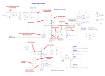
Circuit diagram:
Circuit.png

Circuit elements datasheets:
Q1: JCS4N60 (N-CHANNEL MOSFET)
Q2: A1015 (Transistor PNP)
Q3: C1815 (Transistor NPN)
DW1, DW2: 18-2 (Zener) 17.5-18.3V
D6: HER203 (Rectifier diode)
D12: HER303 (Rectifier diode)
IC1: EL817 (Optocoupler)
IC2: TL431 (Shunt regulator)
IC3: LM78L05 (Voltage Regulator)

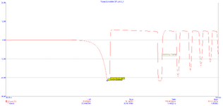
Oscilloscope test for “34V Out”: Vmin 31.7 V, Vmax 35.23 V, Ripple Vpp 3.53 V, Ripple rising time 0.964 mS, Ripple drop time 79.636 mS. "Subripples" on rising stage <1V, about 50kHz;
Vth.jpg
Min output voltage 31.7 V​
Vpp.jpg
Ripple Vpp 3.53 V​
T.jpg
Ripple period 80.6 mS​
Trise.jpg
Ripple rising time 0.964 mS​
Ring.jpg
"Subripples" <1V, ~50kHz​

Here are my questions :

1) How one can theoretically estimate output ripple Vpp?
I made two attempts to calculate it, but my calculations lead to contradiction with oscilloscope data or to energy misbalance (?):
  • Attempt #1 Estimated 0.17 Vpp - far below 3.53 Vpp measured with oscilloscope
Attempt #1 (“Adding ΔE to already stored energy and calculating new voltages”)
Let’s say this power supply unit was powered-on some time ago.​
Total voltage that already exists across EC3 and EC4 (“34V Output”) is threshold voltage settled by shunt regulator and voltage divider, VTH = 34.42 V.​
Taking into account 15:7 winding ratio across EC3 and EC4 and formula E = 0.5*C*V^2,​
EC3 already charged to VEC3Th = 23.47 V and store EEC3Th = 90889 μJ of energy,​
EC4 already charged to VEC4Th = 10.95 V and store EEC4Th = 28177 μJ of energy.​
On next cycle, secondary coils receive ΔE = 1122 μJ of energy in total.​
EC3 receives ΔEEC3 = 765 μJ and EC4 receives ΔEEC4 = 357 μJ (Assuming energy distribution ratio the same as 15:7 winding ratio across EC3 and EC4).​
New energy values on EC3 and EC4 is peak values:​
EC3: EEC3PK = EEC3Th + ΔEEC3 = 90889 μJ + 765 μJ = 91654 μJ, so peak voltage VEC3PK = 23.57 V;​
EC4: EEC4PK = EEC4Th + ΔEEC4 = 28177 μJ + 357 μJ = 28534 μJ, so peak voltage VEC4PK = 11.02 V;​
New “34V Output” voltage is peak voltage VPK = VEC3PK + VEC4PK = 23.57 V + 11.02 V = 34.59 V;​
Ripple peak to peak voltage is Vpp = VPK - VTH = 34.59 V - 34.42 V = 0.17 V​
Far below 3.53 V measured with oscilloscope!​
  • Attempt #2 Estimated 3.38 Vpp - almost as 3.53 Vpp measured with oscilloscope, but it looks like capacitors receiving more energy than it is supplied by coil. Is my attempt #2 somehow correct, or it’s just “drawing the bullseye after firing”?
Attempt #2. (“Adding ΔV calculated from ΔE directly to capacitors”)
Let’s say this power supply unit was powered-on some time ago.​
Total voltage that already exists across EC3 and EC4 (“34V Output”) is threshold voltage settled by shunt regulator and voltage divider, VTH = 34.42 V.​
Taking into account 15:7 winding ratio across EC3 and EC4 and formula E = 0.5*C*V^2,​
EC3 already charged to VEC3Th = 23.47 V and store EEC3Th = 90889 μJ of energy,​
EC4 already charged to VEC4Th = 10.95 V and store EEC4Th = 28177 μJ of energy.​
On next cycle, secondary coils receive ΔE = 1122 μJ of energy in total.​
EC3 receives ΔEEC3 = 765 μJ and EC4 receives ΔEEC4 = 357 μJ (Assuming energy distribution ratio the same as 15:7 winding ratio across EC3 and EC4).​
Now I’m assuming that received ΔE adds ΔV to capacitors as if there is no any previously existing voltage across EC3 and EC4 according to V = (2*E/C)^0.5​
EC3: ΔVEC3 = (2*ΔEEC3/CEC3)^0.5 = (2*765μJ/330μF)^0.5 = 2.15 V, so peak voltage VEC3PK = 25.62 V;​
EC4: ΔVEC4 = (2*ΔEEC4/CEC4)^0.5 = (2*357μJ/470μF)&0.5 = 1.23 V, so peak voltage VEC4PK = 12.18 V;​
New “34V Output” voltage VPK = 25.62V + 12.18V = 37.8 V;​
Ripple peak to peak voltage Vpp = 2.15V + 1.23V = 3.38 V;​
Almost as 3.53 V measured with oscilloscope!​
But now, from E = 0.5*C*V^2, energy stored in EC3 is EEC3PK = 108303 μJ, and in EC4 is EEC3PK = 34863 μJ, or 143166 μJ in total for two capacitors. So it looks like it has been added 24100 μJ of energy (143166 μJ - 90889 μJ - 28177 μJ). But secondary coil supplied only 1122 μJ.​


Calculation of ΔE = 1122 μJ:
Threshold current in primary coil (controlled by Q3)​
VBE(Q3) = IPTh*R6​
IPTh = VBE(Q3)/R6 = 0.7V/0.47Ω = 1.5 A​
Energy stored in magnetic field for threshold current:​
ΔE = 0.5*LP* IPTh^2 = 0.5*997μF*(1.5A)^2= 1122 μJ​
Calculation of threshold voltage VTH = 34.42 V for “34V Output”:
VR11 = VRef(IC2) = VTH*R11/(R14+R11)​
VTH = VRef(IC2)*(R14 + R11)/R11 = 2.495V*(49.9kΩ + 3.9kΩ)/3.9kΩ = 34.42 V​

2) Why did this power module explode? And why epicenter is between cathode of D2 and LF2 Coil?
I tried to check waveforms on right side of C2. I connected oscilloscope probe tip between C2 and R2, and probe ground to D4’s anode (picture attached). After powering module on, master protective fuse in my house fired and switched off electricity in my house… Then I disconnected oscilloscope probe and tried to power-on this module again. This time it exploded with explosion epicenter between cathode of D2 and LF2 Coil.
I estimated that the voltage across these two points should not exceed ~25V induced voltage on Auxiliary coil and very little current because of R2, R1, R7, C2 in this loop, and it should be safe enough… but it looks like I missing some other point.
Before.jpg
Before (with oscilloscope probe)​
After.jpg
Epicenter of explosion​

3) What is the purpose of a dark grey-thin film connected to Aux. coil between insulation tape in transformer?
There was about 5cm dark grey-thin film inside isolation tape wrapped between Primary and Auxiliary coils of transformer, and this film was connected to pin 1 of the transformer with wire. ?
Film.jpg
 

Attachments

  • PowerSupplyUnit.pdf
    16.8 KB · Views: 131
2) You can't connect oscilloscope ground to D4 anode unless you are driving the tested board via an isolation transformer. D2 or D4 (probably D2 in this case) will short one half period of the mains waveform, depending on which of the mains leads are phase and neutral.

3) The film is a shield to reduce capacitive coupling from the primary winding to the aux winding.

Maybe I will have time to look into the ripple calculations.
 
2) Without an isolation transformer, you can use a differential probe. If you want to buy something, get the differential probe. You can get one for $200-$300. It is more useful than an isolation transformer.
 
Hi,

Ripple calculations:
I don't know them by mind, but I expect them to be in every SMPS tutorial and in most SMPS IC datasheets.
Should not be hard to find.

I often use Excel, (each input parameter in an extra cell. Freqyency, inductance, duty cycle ....) so I can easily play around with different conditions.
You may easily even draw charts: for example: ripple_voltage vs duty_cycle.

Klaus
Thank you for reply,
I checked some tutorials for SMPS with duty cycle controlled by some switching IC.
But I gived-up, because, as i understood, in such circuits, ripple voltage is a function of switching frequency and duty cycle, defined by switching IC.
But in my case there is no switching IC, and in contrary, as I understand, switching frequency is function of ripple voltage!
But anyway i'll try to look further into SMPS tutorials.
 
The schematic shows that it's a self-oscillating flyback. Its behavior is governed by three different feedback loops all competing with each other. It looks like you've done an excellent job transcribing the schematic, so I'll do my best to explain how it works.

At power-on, R1 and R7 will gradually pull up Node1 and the gate of Q1, causing it to turn on and energize the transformer via the primary winding (between TR5 and TR3). When this happens, the voltage across the aux winding will also increase. This aux winding output actually couples back to Node1 and Q1, causing Q1 to turn on even more. If Q1 were ever forced to turn off, the aux winding would then create negative voltage at pin TR2, causing Q1 to turn off even faster. So this is one feedback loop, which actually creates positive feedback.

The other two feedback loops are negative, and can override the first positive feedback loop to turn off Q1. When the current through Q1 rises to approximately 1.27A, the voltage at Q1_Source will reach 0.6V, which will start to turn on Q3 via R5.

Q2 and Q3 effectively form an SCR. When either of these BJTs turns on slightly, the pair will "trigger" and will both snap on, effectively shorting "Node1" to zero (relative to the bridge rectifier's negative output). This will cause Q1 to turn off quickly. So basically, R6, R5, Q2+Q3, and R3 form a negative feedback loop which limits the peak current allowed through Q1.

The third feedback loop is the one responsible for regulating the output voltage. The circuit on the secondary side with the TL431 and optocoupler is a very common means of sensing a voltage over an isolation barrier. Basically, whenever 34V rises above ~34.5V, IC2 will conduct current through the LED of IC1. This will cause the primary side phototransistor to sink current into its collector.

At first this current will come from R4 (we'll assume that at the moment, Node1 is high and Q1 is on). But when the voltage across R4 exceeds 0.6V, then Q2 turns on. Like in the second feedback loop, this causes the SCR formed by Q2 and Q3 to trigger, forging Q1 to turn off. The higher the voltage on 34V, the more current IC1 pulls from R4, and the sooner Q1 will shut off, which reduces the energy delivered to the output. This is the final negative feedback loop.

You don't see power supplies built solely out of discrete components very often nowadays. But they're often very ingenious and worth studying for those interested in analog circuits.
 
One overcooked electrolytic cap on the output filter can really
drive ripple voltage up. In a world unconcerned with BOM cost
you'd go for zero ripple at max inductor ripple current. But no
doubt this board had "just enough" (as-shipped) as it's "just
consumer equipment". Extreme ripple voltage might make the
control loop "stay busy" and if you're not lucky this ends up
making output filter charge "slosh" back and forth, scrubbing
energy off through all the series resistances and maybe raising
the losses in devices already stressed. I used to see this affect
wallplug efficiency on converters that had a lot of falling edge
jitter (due to VIN ringing buggering the current mode control
sense comparators, which were rail-referred). If pulse width is
being varied for reasons other than VOUT error, that makes
"slosh" and its compound losses, cycle by cycle.
 
The schematic shows that it's a self-oscillating flyback. Its behavior is governed by three different feedback loops all competing with each other. It looks like you've done an excellent job transcribing the schematic, so I'll do my best to explain how it works.

At power-on, R1 and R7 will gradually pull up Node1 and the gate of Q1, causing it to turn on and energize the transformer via the primary winding (between TR5 and TR3). When this happens, the voltage across the aux winding will also increase. This aux winding output actually couples back to Node1 and Q1, causing Q1 to turn on even more. If Q1 were ever forced to turn off, the aux winding would then create negative voltage at pin TR2, causing Q1 to turn off even faster. So this is one feedback loop, which actually creates positive feedback.

The other two feedback loops are negative, and can override the first positive feedback loop to turn off Q1. When the current through Q1 rises to approximately 1.27A, the voltage at Q1_Source will reach 0.6V, which will start to turn on Q3 via R5.

Q2 and Q3 effectively form an SCR. When either of these BJTs turns on slightly, the pair will "trigger" and will both snap on, effectively shorting "Node1" to zero (relative to the bridge rectifier's negative output). This will cause Q1 to turn off quickly. So basically, R6, R5, Q2+Q3, and R3 form a negative feedback loop which limits the peak current allowed through Q1.

The third feedback loop is the one responsible for regulating the output voltage. The circuit on the secondary side with the TL431 and optocoupler is a very common means of sensing a voltage over an isolation barrier. Basically, whenever 34V rises above ~34.5V, IC2 will conduct current through the LED of IC1. This will cause the primary side phototransistor to sink current into its collector.

At first this current will come from R4 (we'll assume that at the moment, Node1 is high and Q1 is on). But when the voltage across R4 exceeds 0.6V, then Q2 turns on. Like in the second feedback loop, this causes the SCR formed by Q2 and Q3 to trigger, forging Q1 to turn off. The higher the voltage on 34V, the more current IC1 pulls from R4, and the sooner Q1 will shut off, which reduces the energy delivered to the output. This is the final negative feedback loop.

You don't see power supplies built solely out of discrete components very often nowadays. But they're often very ingenious and worth studying for those interested in analog circuits.
Thank you! very clear explaination
 
Hello all

It is second part of this post.
At last I was able to simulate this flyback converter with Micro-Cap 12 and was able to finish my “theoretical” calculation attempt (with help of GNU Octave).
It looks like it solved question regarding enormous output ripple from my previous post, however some new questions regarding this circuit arised.
First I’ll write what I’ve done and then write new questions at the end of this post.

Micro-Cap 12 simulation
I simulated original circuit with these changes/simplifications:
-AC to DC circuity replaced with simple DC power supply;
-5V output circuity deleted;
-CY capacitors deleted;
-MOSFET “VTO” parameter manually set to 4V;
All other circuit elements leaved unchanged (original circuit with links to dataheets is in previous post)
Micro-Cap “.CIR” file attached, just open it with Micro-Cap and run Transient analysis (it will take several minutes to finish).

Here is circuit used in simulation and simulated waveform:
FlybackConverter5.PNG

Circuit used in Micro-Cap simulation​
MicroCap Ripple.png

Ripple waveform simulated by Micro-Cap​

After careful investigation of simulated ripple waveforms, I found that each of “Subripples” actually corresponds to converter’s complete ON/OFF working cycle, but without receiving negative feedback from secondary side (“short” cycle). In other words, It looks like after reaching destignated output voltage, converter fires extra several times before feedback from secondary side puts primary side “on pause”. So output EC capacitors gets more charge than expected.

My own calculations attempt
I was able to calculate simplified working cycle for of this flyback converter step by step, using formulas for series RC/RLC circuits and Octave to solve differential equations.
Also I was able to simulate series of “Subripples” by putting my original calculation into loop and allowing Vref of Shunt regulator to have “hysteresis” instead of one definite 2.495V value.
My calculations and Octave code attached. Just copy-paste and run code in one of on-line octave compilers (for example this one).
Calculated Ripple narrow Vref.png

Ripple waveform with Shunt regulator Vref(min) = 2.48V Vref(max) = 2.52V
(Very similar to Micro-Cap simulated waveform)​
Calculated Ripple wide Vref.png

Ripple waveform with Shunt regulator Vref(min) = 2.298V Vref(max) = 2.554V
(some similar to real waveform captured by oscilloscope)​
Waveforms captured by oscilloscope
Vpp.jpg

Ripple waveform​
Ripple rising.jpg

Zoom at rising phase​

Results

ItemReal flyback converterMicro-Cap simulationCalculation attempt with
Shunt regulator
Vref(min) = 2.48V
Vref(max) = 2.52V
Calculation attempt with
Shunt regulator
Vref(min) = 2.298V
Vref(max) = 2.554V
“34V Out” min31.7 V34.3 V34.2 V31.7 V
Ripple Vpp3.53 V0.43 V0.66 V3.57 V
Ripple rising time964 μS2147 μS963 μS6327 μS
Ripple drop time79636 μS15686 μS11852 μS63442 μS
Total ripple length80600 μS17833 μS12815 μS69769 μS
Subripples Vpp0.2-0.6 V0.11 V0.165 V0.16-0.18 V
Subripple length12-19 μS683 μS316 μS316 μS
Subripples Num~804421

Micro-Cap simulation and my calculations attempt not matches however both produces results of the same order. From another side, they both differs from oscilloscope test result obtained for real converter.
When I allow Shunt regulator to have narrow “hysteresis” for Vref, I obtain waveform similar to that simulated with Micro-Cap.
And when I allow Shunt regulator to have wide “hysteresis” for Vref, I obtain waveform some similar to that real converter produce.
So I’m making conclusion that Ripple Vpp in real converter is so high because of poor performance of shunt regulator and it looks like question my previous post about enormous Vpp of “34V Output” ripple seems to be solved.


New questions:

1)
According to Micro-Cap simulation there is neglible current through diode D6. Charge accumulated in EC3 is always the same as in EC4, so voltages across EC3 and EC4 (and output voltages) depends only on ECs capacitance ratio and not depends on Ls1 and Ls2 turns ratio. So why there is need connection from point between secondary coils and point between ECs via D?

2) According to Micro-Cap simulation and in my calculations, it is need long time to recharge C2 to MOSFET’s gate threshold level at final phase of working cycle (up to 95% of “Subripple” cycle time). But It looks like in real converter, C2 recharges and activate MOSFET very fast, so new cycle starts almost instantly after negative feedback disappears. Maybe anyone have ideas why? Or maybe there is some other process that rechares C2 switches-on MOSFET? For example, maybe ringing that starts after secondary coil demagnetization reflects to auxiliary coil and charges C2 (But it is not the case according to Micro-Cap simulation)?
MicroCap Subripple2.png
 

Attachments

  • FlybackConverter.zip
    13.5 KB · Views: 45
  • OctaveFlybackRippleCalc.zip
    5.1 KB · Views: 43
  • Calculation Attempt.pdf
    338 KB · Views: 50
According to Micro-Cap simulation there is neglible current through diode D6
Apparently you didn't apply a load to 12V or 5V output, otherwise D6 current can't be zero. Without TR8 circuit, 12V and 5V output can't be used. I guess however, it's serving a purpose.
 
The voltage will depend on the secondary inductances, not the output capacitances' ratio.
Calc the volts per turn, and get the voltage like that....but multi coil flybacks are well known for very poor cross regulation.
The thin film is a bit of copper strip inside the insulation tape, it is to shield the primary coil from the secondary, and so reduce common mode emissions.
It sounds like its a hysteretic mode converter....motor boating up and down the output voltage, but within bounds.
What was the power output?...must be small as transformer doesnt look interleave wound...unless they sandwich the primary...and you only have 22uf at primary, so power must be quite low.
Always power circuits through a fuse board, which you can make, and put a very low value fuse there.
To scope ripple its best to do it with a "coaxial probe", which you have to make yourself. Much posts on it in this forum.
As discussed, beware blowing up the scope as scope ground is earth connected.
You can actually make your own diff probe for very cheap....the shop bought ones are hideously overpriced....

...its just an opamp set up in diff mode, with high value input impedances.....and we pay £200 for it !!!
They are hideously noisy, and give very poor, noisy scope traces, and for £200!!!

The discrete flybacks like yours are quite interesting, and , dare i to say it, when the nuclear war happens, and we all blow up each others semico fabs, then we will all be designing our SMPS like this.
In the meantime, for your spec, just put a Tinyswitch in there, or an NCP12xx say, and be done with it.

The reason the discrete flyback ones are so common, is that , as you find, reverse engineering them is time consuming, ,and so the importers woudlnt think they could ever do it themselves...when in fact, they probably could....eg with a tinyswitch....but they dont know about tinyswitch, and they dont know it could do what your cct does.
Some of the discrete flybacks have a dependency on the circuit strays, especially the drain node capacitance, and the leakage inductance, and that makes them much harder to analyze.
 
Last edited:
Apparently you didn't apply a load to 12V or 5V output, otherwise D6 current can't be zero. Without TR8 circuit, 12V and 5V output can't be used. I guess however, it's serving a purpose.
I have tried to simulate this circuit with a load and yes, You are right: indeed there is current through D6 and output capacitor's voltage became
dependt on coils winding ratio. A simple answer after many days of solving this puzzle... now i know that load is necessary to account during simulations/calculations.
 
The voltage will depend on the secondary inductances, not the output capacitances' ratio.
Calc the volts per turn, and get the voltage like that....but multi coil flybacks are well known for very poor cross regulation.
The thin film is a bit of copper strip inside the insulation tape, it is to shield the primary coil from the secondary, and so reduce common mode emissions.
It sounds like its a hysteretic mode converter....motor boating up and down the output voltage, but within bounds.
What was the power output?...must be small as transformer doesnt look interleave wound...unless they sandwich the primary...and you only have 22uf at primary, so power must be quite low.
Always power circuits through a fuse board, which you can make, and put a very low value fuse there.
To scope ripple its best to do it with a "coaxial probe", which you have to make yourself. Much posts on it in this forum.
As discussed, beware blowing up the scope as scope ground is earth connected.
You can actually make your own diff probe for very cheap....the shop bought ones are hideously overpriced....

...its just an opamp set up in diff mode, with high value input impedances.....and we pay £200 for it !!!
They are hideously noisy, and give very poor, noisy scope traces, and for £200!!!

The discrete flybacks like yours are quite interesting, and , dare i to say it, when the nuclear war happens, and we all blow up each others semico fabs, then we will all be designing our SMPS like this.
In the meantime, for your spec, just put a Tinyswitch in there, or an NCP12xx say, and be done with it.

The reason the discrete flyback ones are so common, is that , as you find, reverse engineering them is time consuming, ,and so the importers woudlnt think they could ever do it themselves...when in fact, they probably could....eg with a tinyswitch....but they dont know about tinyswitch, and they dont know it could do what your cct does.
Some of the discrete flybacks have a dependency on the circuit strays, especially the drain node capacitance, and the leakage inductance, and that makes them much harder to analyze.
Thanks for your commenting on this type of converters and for the advice regarding fuse board, caxial probe and diff probe, i definetly will
try to make it. This converter power output is 30W.
 
The schematic shows that it's a self-oscillating flyback. Its behavior is governed by three different feedback loops all competing with each other. It looks like you've done an excellent job transcribing the schematic, so I'll do my best to explain how it works.

At power-on, R1 and R7 will gradually pull up Node1 and the gate of Q1, causing it to turn on and energize the transformer via the primary winding (between TR5 and TR3). When this happens, the voltage across the aux winding will also increase. This aux winding output actually couples back to Node1 and Q1, causing Q1 to turn on even more. If Q1 were ever forced to turn off, the aux winding would then create negative voltage at pin TR2, causing Q1 to turn off even faster. So this is one feedback loop, which actually creates positive feedback.

The other two feedback loops are negative, and can override the first positive feedback loop to turn off Q1. When the current through Q1 rises to approximately 1.27A, the voltage at Q1_Source will reach 0.6V, which will start to turn on Q3 via R5.

Q2 and Q3 effectively form an SCR. When either of these BJTs turns on slightly, the pair will "trigger" and will both snap on, effectively shorting "Node1" to zero (relative to the bridge rectifier's negative output). This will cause Q1 to turn off quickly. So basically, R6, R5, Q2+Q3, and R3 form a negative feedback loop which limits the peak current allowed through Q1.

The third feedback loop is the one responsible for regulating the output voltage. The circuit on the secondary side with the TL431 and optocoupler is a very common means of sensing a voltage over an isolation barrier. Basically, whenever 34V rises above ~34.5V, IC2 will conduct current through the LED of IC1. This will cause the primary side phototransistor to sink current into its collector.

At first this current will come from R4 (we'll assume that at the moment, Node1 is high and Q1 is on). But when the voltage across R4 exceeds 0.6V, then Q2 turns on. Like in the second feedback loop, this causes the SCR formed by Q2 and Q3 to trigger, forging Q1 to turn off. The higher the voltage on 34V, the more current IC1 pulls from R4, and the sooner Q1 will shut off, which reduces the energy delivered to the output. This is the final negative feedback loop.

You don't see power supplies built solely out of discrete components very often nowadays. But they're often very ingenious and worth studying for those interested in analog circuits.
Nice analysis. I pretty much understand everything except for the self-oscillating part.

I attached a marked up the schematic with different section analyzed. How does the circuit oscillate? I assume at startup, the gate of Q1 is pulled up and charged through R1 and R7. This causes current to flow through the primary. As current flows through the primary, a voltage builds up that opposes the flow of current. Due to magnetic coupling, voltage also builds up across the auxiliary and secondary windings according to dot convention. Therefore, the auxiliary voltage of TR2 is positive with respect to TR1. C2 initially looks like a short circuit (0V). As TR2 goes positive, C2 is "shorted" and the gate of Q1 is pulled up to TR2 by R2. This causes the gate voltage to rise quickly which allows more current to flow through Q1 and the primary winding.

Here are my questions:
  • As C2 charges through R2 what happens?
  • What causes Q1 to turn off?
  • What is C3's purpose?

I don't full understand how Q1 turns off initially.

I assume when the auxiliary reverses polarity, a negative voltage is applied across the gate-source of Q1. Therefore, Vgs is negative. Hence, why DW1 and DW2 are there.

Since C2 was originally charged positive, when the auxiliary winding flips polarity and TR2 goes negative, the left side of the capacitor is now negative, compared the right side of the capacitor, and the gate node is even more negative than TR2 due to leftover voltage across C2, sort of like a charge pump. This negative voltage drives Q1 off quickly. So I assume C2 helps turn on/off Q1 quickly.

Is this analysis correct?

Edit: Is Q1's initial turn-off controlled by the current sensing circuit?

When I_Q1*R6 (0.47 Ω)=0.6 V or I_Q1 = 1.27 A, the over-current circuit triggers the SCR formed by Q2 and Q3 and these pull Q1's gate low, initially? Perhaps, this is how the circuit self-oscillates?
 

Attachments

  • Flyback Power Supply.png
    Flyback Power Supply.png
    1.5 MB · Views: 62
Last edited:
Nice analysis. I pretty much understand everything except for the self-oscillating part.

I attached a marked up the schematic with different section analyzed. How does the circuit oscillate? I assume at startup, the gate of Q1 is pulled up and charged through R1 and R7. This causes current to flow through the primary. As current flows through the primary, a voltage builds up that opposes the flow of current. Due to magnetic coupling, voltage also builds up across the auxiliary and secondary windings according to dot convention. Therefore, the auxiliary voltage of TR2 is positive with respect to TR1. C2 initially looks like a short circuit (0V). As TR2 goes positive, C2 is "shorted" and the gate of Q1 is pulled up to TR2 by R2. This causes the gate voltage to rise quickly which allows more current to flow through Q1 and the primary winding.

Here are my questions:
  • As C2 charges through R2 what happens?
  • What causes Q1 to turn off?
  • What is C3's purpose?

I don't full understand how Q1 turns off initially.

I assume when the auxiliary reverses polarity, a negative voltage is applied across the gate-source of Q1. Therefore, Vgs is negative. Hence, why DW1 and DW2 are there.

Since C2 was originally charged positive, when the auxiliary winding flips polarity and TR2 goes negative, the left side of the capacitor is now negative, compared the right side of the capacitor, and the gate node is even more negative than TR2 due to leftover voltage across C2, sort of like a charge pump. This negative voltage drives Q1 off quickly. So I assume C2 helps turn on/off Q1 quickly.

Is this analysis correct?

Edit: Is Q1's initial turn-off controlled by the current sensing circuit?

When I_Q1*R6 (0.47 Ω)=0.6 V or I_Q1 = 1.27 A, the over-current circuit triggers the SCR formed by Q2 and Q3 and these pull Q1's gate low, initially? Perhaps, this is how the circuit self-oscillates?


While waiting for reply from mtwieg
i also have some questions/comments regarding your analysis:

1) As for C4 capacitor. Can you please explain why do you call it "Speedup cap" and what is its role according to your understanding?
As for me, I personally treating C4 (and C3) as "Slow down cap".
Reason is: when I was trying to perform simulation without C3 and C4, sometimes I got error message like "infinities/singular matrix" and warning that this error often caused by fast switching of inductors. So I thought that role of these capacitors is to slow down switching-off process for primary coil. For example to avoid too fast drop of coil current and, therefore, to avoid too high inductive spike.
But I'm not sure about it.

2) Regarding charging of C2 throug R2
You can run simulation of this circuit in Micro-Cap (this software is free now). Zipped file "FlybackConverter.zip" attached in my reply #10 to this thread. Just unzip this file and open this file with Micro-Cap and run Analysis->Transient->Run. C2 voltage graph will be along other simulated graphs in R2C2 subfolder.
According to Micro-Cap simulation, voltage between left and right plates of C2 will be ~4V (threshold Vgs of Q1) at the moment Q1 switcheds on. Before Q1 and primary coil switches off (after about 10uS), induced current from TR2 will flow into right side of C2 via R2 and will decrease C2 voltage to ~1V.
(~5uS and ~1.8V according my "theoretical" calculations)

Actually I have burned this converter (along with fuses in my house) when incautiously used oscilloscope probes trying to find answer for this question...

3) As for initial switching off of Q1 - yes, it is controlled by current sensing resistor R6.
Sorry to hear you burned up fuses! All part of the normal learning process. I can suggest a couple pieces of test equipment that might help when troubleshooting circuits like these. Unfortunately, some of the equipment is kind of expensive. A differential probe for measuring across circuit elements. An isolation transformer to power the AC input switch mode power supply. An auto-transformer or variable transformer. A light bulb in series with the switch mode power supply.

The differential probe is useful for measurement across circuit elements that are "floating" with respect to earth ground. The issue is that the ground lead of a CRT oscilloscope chassis ground inside the oscilloscope. Chassis ground of the oscilloscope is typically tied to earth ground through the AC plug. So when the ground lead is connected to a floating part of the circuit, the ground lead will actually short that node back to earth ground. Shorting the floating nodes to earth can either burn up the scope, the circuit under test, or both.

An isolation transformer keeps the circuit isolated from earth ground. Since the circuit is isolated from earth you can use a normal oscilloscope to probe around the circuit. The isolation transformer can be also be safer (or less safe) depending on you look at it. Since the output of the isolation transformer is isolated from earth ground both AC outputs float with respect to AC mains. There is a chance that if you accidentally touch one leg of the AC outputs you only feel a slight tingle instead of an electric shock. You lose the benefit of a Ground Fault Circuit Interrupter (GFCI) that protects you against AC mains however. Either way, working on any AC can be dangerous, so you still want to always use caution. Please.

The autotransformer or variable transformer allows you to slowly bring the AC input up to voltage. This allows monitoring of current draw and voltage and possibly saving the circuit under test from damage.

The light bulb trick prevents the circuit under test from drawing too much current and blowing up if there is a short circuit. The light bulb essentially provides an AC impedance and limits the amount of current in the event there is a short in the circuit under test.

Here are some helpful links that discuss further:

Your questions:
1) The speedup cap typically helps to turn the BJT on and off quicker. When the capacitor is initially discharged the capacitor looks like a short circuit (0 V). This shorts out and bypasses the resistor. You can think of the speedup cap as a sort of differentiator that allows a spike of current through until the capacitor is charged to the voltage across the base resistor. When the gate (or base drive) drive circuit turns off and goes to ground or negative, the charge left over on the plates of the capacitor cause excess carriers to be "sucked" out of the base of the transistor. This is because when the left side of the capacitor C4 switches polarity and the capacitor still has charge, the right side will be more negative due to the charge on the plates and will attract carriers from the base. Helping turn off the transistor.

Image of the speedup current
1699547496744.gif


2) I would like to take a look at the simulation, I was not aware the voltage of C2 actually went down. That is the opposite of how I understood the circuit. I assumed the auxiliary winding is used for regeneration or positive feedback and C2 charges up through R2. A simplified circuit to the one you are working on is found in cheap USB charges for cell phones. There is a series RC circuit off the auxiliary winding. However the series RC seems to control the on time and frequency of the switching element in the Ringing Choke Converter (RCC). A different circuit topology. The analysis will be somewhat different between the two.
1699548202094.png

--- Updated ---

First off, I want to say you have done an excellent job with this circuit. I want you to pat yourself on the back. This is extremely impressive. Everything you have done.

Regarding the circuit damage, I actually feel bad, I should have mentioned to take care when measuring the voltage across C2 with the oscilloscope. That is my fault.

You should feel good about everything you have worked on and learned during this project. This is difficult, even for people with lots of experience.

With that said, regarding question #2. I believe I see what is happening in the simulation.

As voltage increases across the auxiliary winding, TR2 becomes more positive. As TR2 becomes more positive C2 is charged through R2. The current through C2 and R2 flows into the gate capacitance of Q1. The current charges the gate-source capacitance which quickly raising the gate voltage above the threshold voltage (Vth). This current quickly turns on Q1.

A quick rise in current flows through Q1 from drain-source and hence through the primary of the transformer. Once the current raises the voltage of R4 to ~0.6 V. The current sensing/overcurrent circuit, formed by Q2 and Q3, turns on.

When the SCR formed by Q2 and Q3 turns on, Q1's gate and source are shorted together by the SCR. As Q1's gate charge is dissipated through the SCR, Vgs lowers below the threshold voltage, Vth, which turns off Q1. The left side of C2 is pulled low by the SCR as well. The SCR shorts out the optocouper collector circuit (IC1_4, R4 and R3), places C2 and R2 directly across the auxiliary winding. While Q1 turns off, C2 raises every so slightly more by the auxiliary winding voltage. Once the current through Q1 reduces, the primary winding reverses voltage attempting to keep current flowing in the same direction. This induces a reverse voltage across the auxiliary and secondary windings due to magnetic coupling of the transformer. Energy from the primary is dumped into the auxiliary and secondary during this time.

The reverse in voltage across the auxiliary discharges C2 through R2 and reverses current across C2 and R2, which helps turn Q1 off quickly. The reverse voltage across the auxiliary also places a negative voltage across the gate-source of Q1, hence Vgs goes negative. This is why zeners DW2 and DW1 are there, to protect Q1 max gate-source rating of Vgs = +/- 30V.

Note that this all happens very quickly in the simulation, tens or hundres of microseconds.

As you can see in the simulation, once the voltage across R4 is ~0.6 V the SCR circuit triggers.

1699554634031.png

1699554694504.png

1699554746316.png

1699554929072.png

1699555010233.png


Let me know if you have any more questions. I will try my best to help.
--- Updated ---

To sum up my previous post and answer your question #2. It is the current sensing/over-current circuit that is turning on and stopping the charge into C2.
1699556027756.png
 
Last edited:
One interesting note is that there is a small drop-off in current through R2. The small drop-off occurs before the SCR is triggered. The drop-off I believe is due to zener diodes DW1 and DW2 conducting and clamping the gate-source voltage of Q1, which is essentially Vaux.

1699557830242.png

1699557952558.png


Edit: I'm not 100% sure though. This is just my guess.
 

Attachments

  • 1699557932815.png
    1699557932815.png
    66.9 KB · Views: 57
  • 1699557939916.png
    1699557939916.png
    66.9 KB · Views: 49
Bad guess, the auxiliary voltage is due to the primary voltage when Q1 turns on. Did you make the transformer model?
1699572664955.png
1699572586421.png
 
Last edited:
Bad guess, the auxiliary voltage is due to the primary voltage when Q1 turns on. Did you make the transformer model?View attachment 186166View attachment 186164
Thank you for your detailed answer and for your time spent analysing and explaining simulation result.

Regarding circuit damage - sorry for misunderstanding - it is absolutely not your fault!
I have burned it long time ago - just before starting this thread, long before you posted here.
I mean that time I also was interested in charging of C2 through R2.

I needed to search for article about troubleshooting of SMPS as in link you provide before starting this project...

As for transformer model - I didnt make detailed model, in a sense that I dint take into account wire gauges, physical sizes etc.
I have measured primary coil inductance with RLC meter and then re-calculated other coil's inductances according Lp/(Np/Nx)^2 ratio and
then used obtained inductances using K1 magnetic core model for simulation.

I'm not sure weather I should have use actually measured inductances instead of calculated in respect to Lp during simulation?
Actual measured (not calculated) inductances was Laux = 9.7uH (instead of 7uH), Ls1 = 48uH (instead of 43uH), Ls2 = 16.8uH (instead of 9uH).
 

LaTeX Commands Quick-Menu:

Similar threads

Part and Inventory Search

Welcome to EDABoard.com

Sponsor

Back
Top