Continue to Site

Welcome to EDAboard.com

Welcome to our site! EDAboard.com is an international Electronics Discussion Forum focused on EDA software, circuits, schematics, books, theory, papers, asic, pld, 8051, DSP, Network, RF, Analog Design, PCB, Service Manuals... and a whole lot more! To participate you need to register. Registration is free. Click here to register now.

Design of 4 way Wilkinson power divider: Split power to 4 antennas with Wilkinson power divider

Status
Not open for further replies.

Jonas1893

Newbie level 4
Joined
May 11, 2022
Messages
6
Helped
0
Reputation
0
Reaction score
0
Trophy points
1
Activity points
58
I am still inexperienced with Microwave Engineering and therefore have a few questions regarding the Wilkinson power divider. As mentioned in the title I would like to design a 4 way Wilkinson power divider to split power to 4 antennas with the Wilkinson power divider.
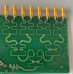
First I want to simulate it with the software ADS and then build it. Now I am not sure how the general structure of a 4 way Wilkinson is. Do I have to split 2 ways first and then split 2 ways again in both ways so that I have 4 as shown in the 1st picture or can I directly split all 4 lines (see drawing in the 2nd picture). There is a lot of literature about the 2:1 power divider but I can't find much about the 4:1. And do I have to use such a circle or is it also possible to use straighter lines?

1.
4_1.jpg

2.
1652440162724.jpeg
 

In case of doubt, I'd refer to the cascaded topology of picture 1. Picture 2 is missing resistor symmetry. 4 resistors with a common star point should work, but that's difficult to implement as a planar structure.
 

I will leave the resistors out. My professor said that I will not need them for my application to simplify the circuit.
 

But do I have to do it like in the first picture?
Your design is not correct. Typical N-Way Wilkinson Dividers is as follows. There are some other academic purpose wideband/high isolation approximations but this is generic one.
1652448874389.png
 

Ok, do you know how to implement it in ADS? I started defining my MSUB with all the material constants. But now I'm not sure how to do the design. I have 100 Ohm for the first part when they split and after this I have 50 Ohms. Do I need two different MSUB for 100 and 50 Ohm? And where do I have to place them?
 

I'd refer to the cascaded topology of picture 1.

I agree with FvM. Attached is a photo of a cascaded Wilkinson project from the 1990s, freq range 900MHz - 2100MHz. Two stages for each Wilkinson divider used here for wider bandwidth.
--- Updated ---

I started defining my MSUB with all the material constants.

That is correct. One substrate material means one MSUB block. The line width for different line impedance is set in the MLIN elements. To calculate width, you can use the LineCalc tool in ADS, this is available from the Tools menu in schematic window.
 

Attachments

  • wilkin8.jpg
    wilkin8.jpg
    172 KB · Views: 210
Last edited:

Ok, yes I calculated it with LineCalc. I think that should be correct. I started arranging the components in the schematic. Can I send you my schematic if I have any qustions?
 

I will leave the resistors out. My professor said that I will not need them for my application to simplify the circuit.
That's possible if you expect no reflections from the output ports or don't need to hinder it from propagating to the other outputs. Without the resistors as shown in post #6 it's not strictly a Wilkinson divider.
 

Status
Not open for further replies.

Part and Inventory Search

Welcome to EDABoard.com

Sponsor

Back
Top