Continue to Site

Welcome to EDAboard.com

Welcome to our site! EDAboard.com is an international Electronics Discussion Forum focused on EDA software, circuits, schematics, books, theory, papers, asic, pld, 8051, DSP, Network, RF, Analog Design, PCB, Service Manuals... and a whole lot more! To participate you need to register. Registration is free. Click here to register now.

Why is the output of the power divider I designed unstable?

Singkwan

Newbie
Joined
Dec 11, 2023
Messages
2
Helped
0
Reputation
0
Reaction score
0
Trophy points
1
Activity points
32
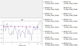
All power dividers shown as below figures have equal power distribution. Why is the output of the power divider I designed unstable? The S parameter exhibits wave like fluctuations.

Drawing1.jpg


Drawing4.jpg
 
Looks ok to me.. But if its unacceptable for your application, I have few ideas:
1) Single divider still has mismatch. Have you tried to simulate single divider? If there is some small mismatch, it will work as 4 impedance transformers (e.g., path from port 1 to port 2). Try to simulate single divider by extending input port length by 90 degree (quarter wavelength) line and compare with unmodified one
2) I never worked with Ansys, but if it uses process called "Meshing", your grid size may be too coarse. Maybe your simulator used lower resolution grid because of larger PCB area. You need to check it by using some option to view generated finite element grid and see if your power divider geometry is still ok.
In my opinion, these "waves" are result of unwanted impedance transformation, and it repeats each n*180 degrees, when your frequency goes from 24GHz to 34GHz, phase length gradually "shrinks" and increases phase length of transmission lines.
 
Hi,

I´m not an expert, but when you start at input #1, then go left to the next divider.
This divider has two branches: On feeds 4 outputs: #2, #3, #3 and #4 while the ther branch feeds 2 outputs only #5 an #6.

now if the power is divided equally to each side, then the left side power is fed to 4 outputs, while the right side is fed to 2 output ...
so in the left case: power/4 and the right sied: power/2
Thus I guess the power at #6 and #7 is about twice the power of #2 to #5. so a plus of 3dB.

Klaus
I thought the same at first, but then I've realized that OP is more advanced and probably understands that. Most likely it is about... pass band ripple of this divider? Maybe there is a better term for microwaves.
 
Looks ok to me.. But if its unacceptable for your application, I have few ideas:
1) Single divider still has mismatch. Have you tried to simulate single divider? If there is some small mismatch, it will work as 4 impedance transformers (e.g., path from port 1 to port 2). Try to simulate single divider by extending input port length by 90 degree (quarter wavelength) line and compare with unmodified one
2) I never worked with Ansys, but if it uses process called "Meshing", your grid size may be too coarse. Maybe your simulator used lower resolution grid because of larger PCB area. You need to check it by using some option to view generated finite element grid and see if your power divider geometry is still ok.
In my opinion, these "waves" are result of unwanted impedance transformation, and it repeats each n*180 degrees, when your frequency goes from 24GHz to 34GHz, phase length gradually "shrinks" and increases phase length of transmission lines.
Thanks a lot, [B]Georgy.Moshkin[/B].
I apologize for any confusion caused by my previous question, as English is not my native language. As you mentioned, my concern revolves around the S-parameters of a power divider exhibiting passband ripple within the 24-34GHz frequency range. I am designing a power divider, just like what [B]KlausST[/B] mentioned, where the output power difference between ports #2-5 (#10-13) and ports #6-9 is maintained at 3dB. However, across the entire frequency band, the power difference between these port groups fluctuates between 2.5dB and 5dB. I am seeking to achieve a smoother output power, as the power divider will later connect to an antenna for testing purposes."
 
It's overoptimistic to expect that the simple geometry works as ideal power divider.

First question, how did you design it and why are you sure that the impedances are perfectly matched?
Secondly, there's a certain amount of coupling between the transmission lines through freefield that modifies the transfer characteristic.
Finally, I guess the divider network is intended as antenna array driver. Are you aware that reflections from individual antennas will produce much worse deviations from designed behaviour?
 
Most probably is about coupling between transmission lines, and EM simulator HFSS is showing this response.
If you do the same simulation using a linear simulator (which don't take into account the coupling between lines) you will get the same response for all Sn1 plots (as is shown in the example attached).
 

Attachments

  • 16port_divider.jpg
    16port_divider.jpg
    100.2 KB · Views: 52
Last edited:
Because your combiner/divider is not symmetrical. If you look at the branches' length, you will see they are not equal. Therefore there are differences between the ports.
You have to place extra transmission lines for the ports 6....9 to compensate the all lengths equal.
A beter option is to use 16 ports in order to get more symmetrical layout. ( or 8 )
 

LaTeX Commands Quick-Menu:

Part and Inventory Search

Welcome to EDABoard.com

Sponsor

Back
Top