Continue to Site

Welcome to EDAboard.com

Welcome to our site! EDAboard.com is an international Electronics Discussion Forum focused on EDA software, circuits, schematics, books, theory, papers, asic, pld, 8051, DSP, Network, RF, Analog Design, PCB, Service Manuals... and a whole lot more! To participate you need to register. Registration is free. Click here to register now.

compatibility of A/D converters.

Status
Not open for further replies.

liteon

Full Member level 2
Joined
Oct 13, 2010
Messages
149
Helped
27
Reputation
54
Reaction score
27
Trophy points
1,308
Location
PAKISTAN
Activity points
2,510
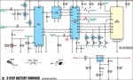
Hi, I need to build a charger for high capacity lead acid battery.It is a three stage battery charger for both low and high capacity batteries.Seem good choice to me,So i checked the market before starting the project and found almost all components except A/D converter TLC548,i can get ADC0831 which is same package (8-pin Dip).But it not pin compatible which is not a bigger problem.The circuit is controlled by a PIC chip , a 2-ch analogue multiplexer-demultiplexer performs monitoring of battery status and feeds it to A/D converter and data is received by the PIC chip.
Can i use the ADC0831 in place of TLC548.
Do i need to re-write the code for PIC in case i use ADC0831?
 

And here is the assembly code for PIC.
 

Attachments

  • bcharg3.txt
    81 KB · Views: 42

There are some minor differences between data acquisition process for each circuit. Maybe need to change code in order to read the data output in the correct manner.

The conversion cycle, which requires 36 internal system clock periods (17 ms maximum), is initiated with the eighth I/O clock pulse trailing edge after CS goes low for the channel whose address exists in memory at the time.
The most significant bit (A7) is automatically placed on the DATA OUT bus after CS is brought low. The remaining seven bits (A6–A0) are clocked out on the first seven I/O clock falling edges. B7–B0 follows in the same manner.

**broken link removed**


When the conversion begins, the output of the SAR comparator, which indicates whether the analog input is greater than (high) or less than (low) each successive voltage from the internal resistor ladder, appears at the DO line on each falling edge of the clock. This data is the result of the conversion being shifted out (with the MSB coming first) andcan be read by the processor immediately.
7. After 8 clock periods the conversion is completed. The SAR status line returns low to indicate this 1⁄2 clock cycle later.

**broken link removed**
 

If i would understand A/D converters i would figure it out myself.I only reason for asking the help is the first time encounter with A/D converters.
So the code is posted already and the control part of hard ware is attached herewith.
Please ....i need it so badly.
 

Attachments

  • 103191_4mg.jpg
    103191_4mg.jpg
    53.6 KB · Views: 62
Last edited:

There are some things you need to change in the program, for example this part:
DEL_CNV
decfsz CYC_AD,f ; keep clock low for 36 internal clocks of TLC548/9
goto DEL_CNV
goto CK1_s
related to the 36 internal system clock periods required for conversion in the case of using TLC549, reduced now at 8 clock period.
 
  • Like
Reactions: liteon

    liteon

    Points: 2
    Helpful Answer Positive Rating
After a lot of search in market i was able to find tlc548.So now there is no need to alter the code which is too long to re-write it.
Thank you all for your time.
 

Status
Not open for further replies.

Part and Inventory Search

Welcome to EDABoard.com

Sponsor

Back
Top