Continue to Site

Welcome to EDAboard.com

Welcome to our site! EDAboard.com is an international Electronics Discussion Forum focused on EDA software, circuits, schematics, books, theory, papers, asic, pld, 8051, DSP, Network, RF, Analog Design, PCB, Service Manuals... and a whole lot more! To participate you need to register. Registration is free. Click here to register now.

CMOS inverters used as drivers

Status
Not open for further replies.

AMSA84

Advanced Member level 2
Joined
Aug 24, 2010
Messages
577
Helped
8
Reputation
16
Reaction score
8
Trophy points
1,298
Location
Iberian Peninsula
Visit site
Activity points
6,178
Hi guys,

I am using a chain of inverters to drive a power mosfet. Those drivers must process the driving signal at very high frequency.

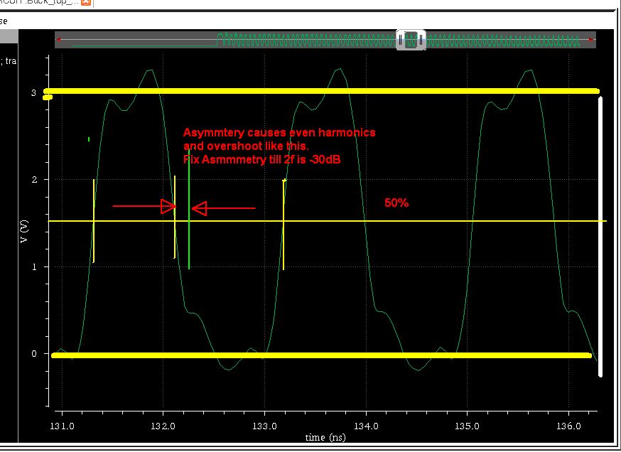
One problem that I am facing is that the signal at the output of each of the inverters have a large peak, looking like an inverter hyperbola with that peak voltage reaching the house of 3.7V.

Does anyone knows what might be causing this?

wave.png
 

Often you see some peaking right before transitions due to capacitive feedthrough from the input to output of the inverter. Once you put a capacitive load on the output it should decrease the peaking though.
 

Well, because this is a chain of inverters and is driving a power mosfet, the capacitance at the output put of each inverter is the next inverter and so on until the power mosfet. I can't do much there.

Is there any tech to remove those peaks?
 

Capacitive feedthrough can surely happen. I would expect "buffered" inverters being used in the test, if so there won't be much feedtrhrough left.

For me, the waveform looks more like caused by trace inductance and ground bounce, in combination with input capacitance of the next stage.

Finally, how are the waveforms captured? 500 MHz signals can be only reproduced with active or resistive probes.
 

All this waveforms are form cadence simulation, and as FvM, considering wire-bondings and stuffs.

You think that this can be happening because of wire-bonding connections? It can be a resonance?

EDIT: FvM, can you explain what you mean by " I would expect "buffered" inverters being used in the test, if so there won't be much feedtrhrough left"?

Capacitive feedthrough can surely happen. I would expect "buffered" inverters being used in the test, if so there won't be much feedtrhrough left.
 

"Buffered" inverter means a three-gate circuit.

Now, as you clarify that this is a simulation. Why don't you take the chance to find the reason for overshoot etc. in your simulation results? It's all at your fingertips, we have about to no information.
 

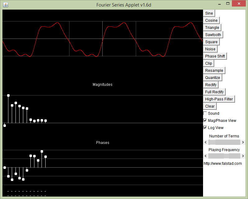
From reviewing your photo, it appears your signal is ~526 MHz with 45% duty cycle and thus even harmonics as strong as odd harmonics up to 3~4Ghz

1) Asymmetry is could be improved.
2) don't worry about peaks IF you are not worried about 1) . This is normal for asymmetry drive impedance and non-linear C load.
3) if 1) is a problem use pullup R to 3V of 5% of nominal source impedance (ESR or RdsOn) to increase duty cycle to 50% at desired threshold or some other improved impedance match termination with lower R at 1.5V

3971679000_1426663511.png


Source impedance of ALCV2 for example is around 10Ω when one examines VI drop at rated current.
 

Hi FvM and sunny.

Thank you guys for the reply. To be honest I have tried to find out what's causing this peaking. I think it might have to do with the bonding wires. Because the power devices VDD is the same as the driver section, this might be related. what happens in the power devices reflects in the driver section. What is interesting is that the VDS of the NMOS has somehow the same shape of that waveform shown.

Sunny, what is the asymmetry that you are referring to?
 

If you are talking about a standard power MOSFET then
500MHz is way overclocking it. Few RD LDMOS, even,
purport to be suited to that frequency range.

MOSFET gate charge has complex behavior (Miller
plateau, once drain begins to slew, etc.) and I doubt
you can resolve this when toggling the gate so fast.
If you want understanding, I suggest you work back
from a more leisurely frequency that lets things fully
settle, and then increase it looking at how various
"features" eventually combine in short-time.
 

I see. Thank you for you explanation.

Taking the advantage of this post, does anyone knows how can I estimate the delay of a general closed loop feedback system, or in this case, in particular from a dc-dc converter?
 

Status
Not open for further replies.

Part and Inventory Search

Welcome to EDABoard.com

Sponsor

Back
Top