Continue to Site

Welcome to EDAboard.com

Welcome to our site! EDAboard.com is an international Electronics Discussion Forum focused on EDA software, circuits, schematics, books, theory, papers, asic, pld, 8051, DSP, Network, RF, Analog Design, PCB, Service Manuals... and a whole lot more! To participate you need to register. Registration is free. Click here to register now.

CMOS Class B Amplifier

Status
Not open for further replies.

dshoter13

Member level 4
Member level 4
Joined
Oct 20, 2014
Messages
72
Helped
4
Reputation
8
Reaction score
4
Trophy points
8
Visit site
Activity points
619
RF CMOS Power Amplifier Design - Virtuoso

Hi. I'm trying to design a CMOS Class B PA using Virtuoso. I designed my output matching network for maximum gain.. but when I'm simulating S-Param, Harmonic Balance and doing Periodic States Simulations etc, I have to use a Port, and It comes with 50Ohm resistence. My question is: it will have impact in my PA performance? Do I have to design a input matching network to obtain the correct results in Virtuoso?


Thank you all for you attention.

Best regards.

- - - Updated - - -

Sorry, I design a very simple low-pass matching network (ideal elements) and it boosted the PAE and Output Power.

Thank you all for you attention.
 

Re: RF CMOS Power Amplifier Design - Virtuoso

Since the the matching circuit has been defined, why don't you implement this on your schematic ?? I presume that you have already defined optimum load and source for this PA.So, design the matching circuits that matche these impedances to 50 Ohm standard port impedance..
I didn't understand what your problem is..
If your question is that if you use port element with 50 Ohm instead of optimum impedances, will it impact the performace?? Yes surely it will.But you can also place these "port" elements without any matching circuit but filling resistance and reactance field with your values which you have already found for max. power.It runs too..
 
Re: RF CMOS Power Amplifier Design - Virtuoso

Yes, exactly.. But since I'm working in Integrated Environment, I won't need to design an input matching network.. but for the sake of measures, I have to "adapt" the port to my NMOS, either way.

Thank you very much.
 

Power Amplifier - Virtuoso 6.1.15

Hi.

I'm designing a Power Amplifier in Virtuoso. I'm currently following a Power Amplifier WorkShop from Cadence (PDF in their documentation), and I'm having trouble when I try to do the Load-Pull simulation.
I'm doing exactly what they describre in their WS, but in their screenshots two "magic" variables appear (mag and phi), that I don't know where they come from.. I think that the ADE L should do that automatically, but I'm not getting nothing from it. I'm doing a Harmonic Balance, and in the last checkbox (loadpull counters) when I check, it should show me those variables.. But I'm not getting them..

Anyone has ever done load-pull measurements? Any idea?
 

Re: Power Amplifier - Virtuoso 6.1.15

Hi,

I guess these magic variables come from your load-pull port (I don't remember how exactly it names, because I don't have rfLib for now) and these variables just polar form of your load impedance.
 

Re: Power Amplifier - Virtuoso 6.1.15

Hi,

I guess these magic variables come from your load-pull port (I don't remember how exactly it names, because I don't have rfLib for now) and these variables just polar form of your load impedance.

That would be true for older versions of the software, but in recent versions (like mine) we do not need that special port..
I have looked in rfLib for that, but it is not there.. I checked in other places, and everyone says (just like in the WorkShop PDF) that I do not need to use thath..
 

Re: Power Amplifier - Virtuoso 6.1.15

This doesn't depend from virtuoso version, but from MMSIM version. I have MMSIM 13.1 and there is tutorial for load-pull:
 

Attachments

  • loadpull.pdf
    974.8 KB · Views: 92

Re: Power Amplifier - Virtuoso 6.1.15

This doesn't depend from virtuoso version, but from MMSIM version. I have MMSIM 13.1 and there is tutorial for load-pull:
Thank you very much. I was following other workshop, but this one gives me the same errors.. I get simulation errors because my triplexer does not have PortAdapter.. This component is missing in my rfLib.. Any idea?

Thank you very much.
 

Hi.
I'm trying to design a Class B amplifier in Virtuoso.
I sized my transistor (N type) so it could deliver a maximum Id current of approx. 535 mA. I'm working with 1.2V, and I followed the Load Line Theory, so I adapted the OutPut with a simple low-pass network so it would transform the 50Ohm load into 3.4Ohm resistance needed in order to ensure Maximum Output Power (Ropt = 2*(Vdd-Vg)/Imax).
Now, I pretend to adapt my input, but I'm having trouble measuring the impedance into the gate of the transistor. I'm plotting S parameters (small-signal approximation) with Pin = -5 dBm, which is the Reference point of Operation that I expect. But when I do the S-parameters calculations, I see that my S12 is above -20dB, so I cannot approximate my input reflection coefficient ~S11..
I tried to run some transient simulation, and I see a very odd thing happening: When I apply a 2.4GHz signal in at input terminal, the signal that I get at the Gate of the transistor is "amplified", what I think that suggests that the amplifier is unstable.
View attachment Vin_Vg.pdf.
After checking this, I check S11 again, and it confirmed that the transistor is Unstable:
View attachment S11_mag.pdf

What I'm trying to understand, is what I should do in order to get a good match in the input, so I can reach a good PAE.. For now I'm using every inductors and capacitors from the analogLib, except the inductors at DC level (RF chokes).
Also, I'm applying the Vg at the gate of transistor using a RF choke.. I do not know if it is the ideal thing to do.. In some articles I see resistances at the gate to do the biasing..

Sorry for the long post, but any help is going to be useful..

Sorry for my english.

Again, thank you all for you attention.

With best regards.
 

From your scope traces, it appears that you are applying a sine wave at the input, and you are getting a distorted sine wave at the output.

Looking at the positive and negative half of the waveform. The output is non-symmetrical. The transistors act like they are mismatched.

The input and output cross 0V at different points in the sinewave.

The negative waveform looks healthy through the entire range from 0V to -1.5V

The positive waveform only looks strong until the 0.3V mark. Then it's as though the bias suddenly went weak. Output only reaches +1.1 V.

The screen that I put here is from both waves at the input. Vg is the wave form at the gate of the transistor, and Vin is the sine wave at the Source Terminals..

I will let here more info:
My schematic:
Screenshot.png

Z-parameters for getting Zin ( pin = -5 dBm) with output for maximum match (Load Line Theory):
View attachment Z-parameters_output_MatchPower.pdf

and here the S-parameters for the same conditions above:
View attachment S_params_MatchPower.pdf

When I plot B1f and Kf I get both above zero from 1GHz to 4GHz. But with the values that I get in Z-parameters, applying the equations to obtain Zin, I'm getting my impedance negative, which tells me that my Amplifier is acting like an oscillator.. Any ideas?

- - - Updated - - -

Sorry, the pdfs are with incomplete information.
Z parameters with output matched for maximum power:
Z_parameters_MatchOut.png

S- parameters under the same conditions:
S-parameters_MatchOut.png
 

I'm facing a problem.. With Idmax of 166mA, the maximum output power until it clips is about 9dBm..
I scaled my transistor and it gives approximately 1000mA, and I did a parametric in the resistance at the drain.. My ouput power won't go any higher that 10 dBm... what's wrong?
 

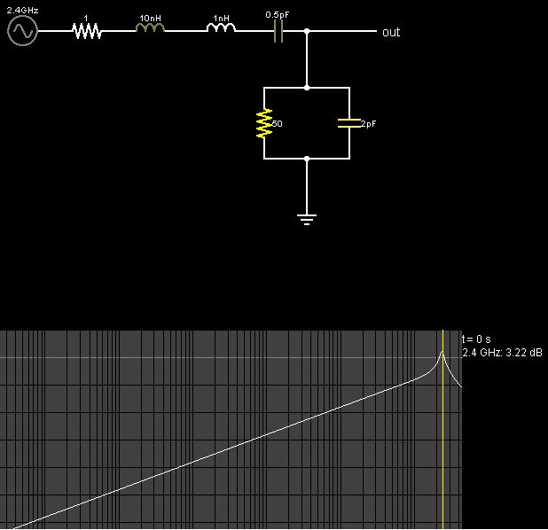
You can get a bunch more just by tuning the reactance and s parameters for 2.4GHz instead of much lower.

Change 20 nH etc for 45 Ohms then LC series for 2.4GHz @ 5 Ohm series impedance into 50 Ohm load.

- - - Updated - - -

Did I do this right?

5856293000_1427147443.jpg


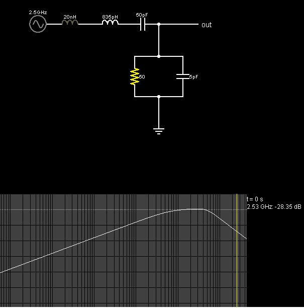
Your filter below.
8586083500_1427147443.jpg


Maybe I didn't model the FET properly when conducting average current.

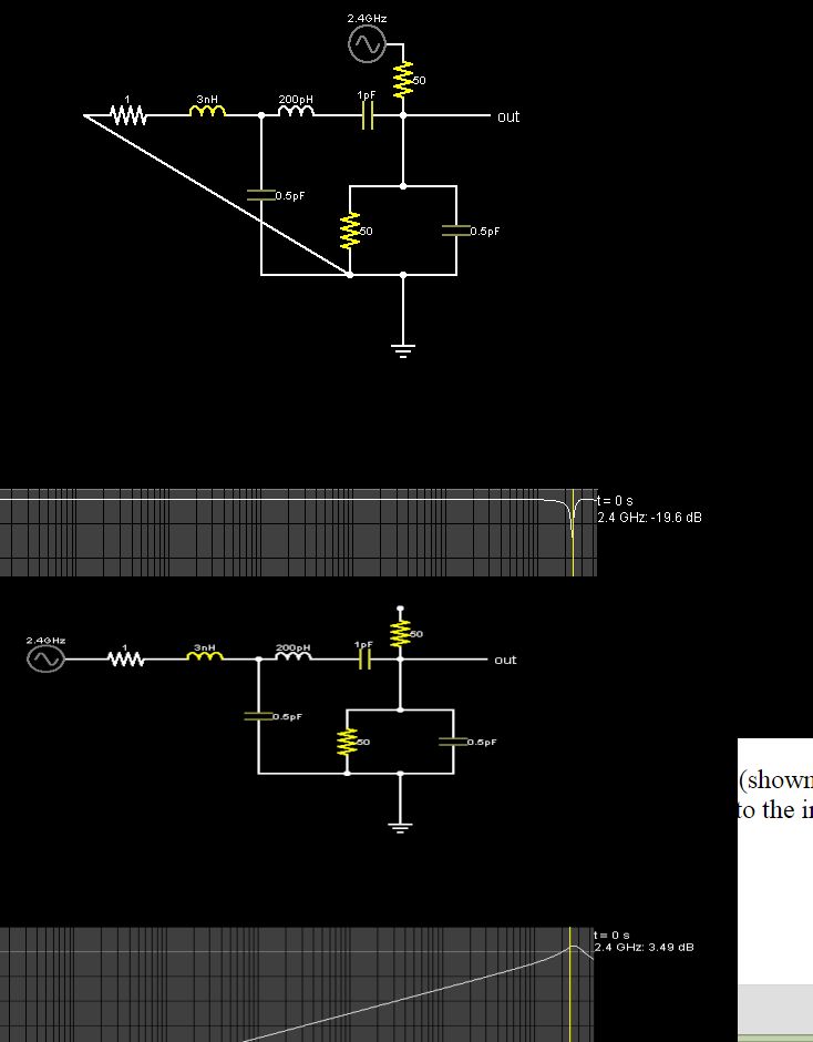
Tweak peak with smaller choke with air core and bigger one precision..

- - - Updated - - -

Take 2

7980290200_1427148348.jpg
I'm sorry, I did not understand the first part..

"Change 20 nH etc for 45 Ohms then LC series for 2.4GHz @ 5 Ohm series impedance into 50 Ohm load."
If I do this, how it is going to boost my output power? And I do not understand what you mean by 2.4GHz @ 5 Ohm series impedance into 50Ohm Load.. I already have 50 Ohm load (my antenna)..
 

Status
Not open for further replies.

Part and Inventory Search

Welcome to EDABoard.com

Sponsor

Back
Top