jimito13
Advanced Member level 1
Dear Forum Members,
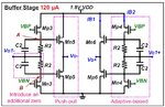
These days i am going through the paper with title : A 2.3mA 240-to-500MHz 6th-order Active-RC Low-Pass Filter for Ultra-Wideband Transceiver (Le Ye, Huailing Liao, Congyin Shi, Junhua Liu, and Ru Huang - IEEE Asian Solid-State Circuits Conference November 8-10,2010 / Beijing, China).
I need some clarification for the voltage buffer they present in their work.I am uploading the respective image that depicts the circuit they have designed for the voltage buffer.
Can somebody tell me what kind of transistors are the Mn5,Mp5,Mn3,Mp3?I mean which of them are nmos and which of them are pmos?
Thanks in advance for any helpful contribution.
Best Regards,
Jimito13