Continue to Site
Follow along with the video below to see how to install our site as a web app on your home screen.
Note: This feature may not be available in some browsers.
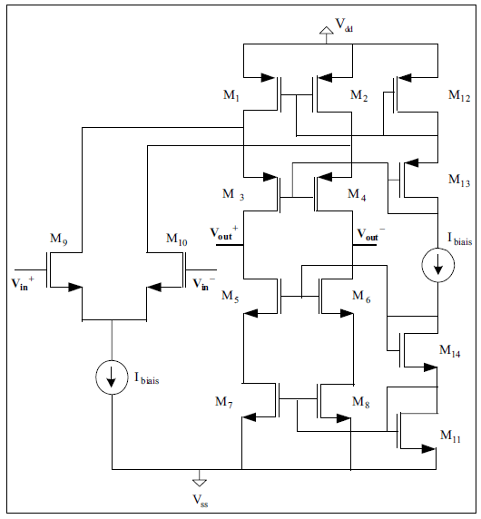
i am using 0.18um tech..
my specifications are
Gain = 60 dB
UGF = 500Mhz
CL = 0.1 pf
Vdd = 1.8V
now from where i have to start??
how can i start calculations of W/L??
See David M. Binkley "Tradeoffs and Optimization in Analog CMOS Design"
Chap. 5: Design of CMOS Operational Transconductance Amplifiers Optimized for DC, Balanced, and AC Performance.
Chap. 5.5: DESIGN OPTIMIZATION AND RESULTING PERFORMANCE FOR THE CASCODED OTAS
Chap. 5.5.1.2: AC optimization
You'll find there an optimization procedure for cascoded OTAs incl. MOSFET dimensioning in 0.18µm tech. Even if the highest frequency "ac" example doesn't meet your requirements re. gain & UGF (gain=56dB, UGF≈60MHz, with currents of 100µA) I think you can profit from the method.
Sure, why not?... the model used is EVK, does it suit for BSIM?