Continue to Site

Welcome to EDAboard.com

Welcome to our site! EDAboard.com is an international Electronics Discussion Forum focused on EDA software, circuits, schematics, books, theory, papers, asic, pld, 8051, DSP, Network, RF, Analog Design, PCB, Service Manuals... and a whole lot more! To participate you need to register. Registration is free. Click here to register now.

[SOLVED] Big EMI issue on LCD screen

Status
Not open for further replies.

flote21

Advanced Member level 1
Joined
Jan 22, 2014
Messages
411
Helped
1
Reputation
2
Reaction score
3
Trophy points
1,298
Activity points
5,595
Hello guys,

I have designed a display board to interface LVDS signal coming from a camera to parallel RGB interface LCD screen input.

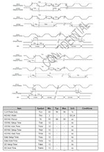
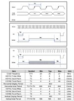
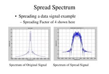
The displayboard does not have any EMI problem. However when i connect it to the LCD screen thought a flat cable, a big EMI interference is coming out of the flat cable. The frequency of this EMI is at 25MHz and it has harmonics every 25MHz up to 700MHz. The 25 MHz is the pixel clock of the RGB data

I tried to reduce the EMI changing the values of the series termination resistors, i added more bypass capacitors, i place finger contacts to have more direct gnd contacts between the LCD screen and the display board....and i got some improvements but still the EMI levels are high.

Any idea to improve the current EMI results?

Thanks in advance.

Greetings
 

Hi,

We miss the informations about your FPGA.
Maybe it already contains a stread spectrum clock (PLL). How can we know?

I don't know whether there is a "individual" spreading on the signal pins. I guess not.

So if you do (PLL) clock spreading you still have 26+ lines switching state on the same time.
This might reduce EMI radiated noise peaks, but does not improve signal integrity.

You wrote you get image problems when adding filters. This tells me that you are at the edge of regarding timing.

So my idea:
* first look for the timing requirements of the LCD (to know how much and in what direction you can vary RGB signals wrt. Pixel_clock) ... and show us
* then tell us about your FPGA timings of RGB signals and pixel_clock .... and FPGA system_clock
Depending on the timings, one posdible solution may be to delay the pixel_clock (by multiples of system_clock_periods/2) to get more relaxed timing for the LCD. Then you may add filters (or just higher ohmic series resistors) to the signal lines to reduce the signal_current and thus the GND_current.

We definitely need more details. When I said we need to see the PCB layout, I did not mean photos if the PCB, I rather thout of the signal and ground routing. The photos don't give much informations, not even about sizes.
When I said you should check datasheets for timings, I rather expected values about setup and hold times w.r.t. FPGA timing than goot/not good information.
Don't get me wrong: if give us values, we have the chance to validate and comment them. If you give "good" we have to rely on this, but cant judge the timing.

Indeed I miss timing diagrams (even hand drawn), scope pictures, timing requirements ... from both: FPGA and LCD to know where are the limits and where and how much we can "adjust".

Klaus
 

Spreading the spectral width of the clock is a game you play to pass a test without changing the amount of EMI put out in fact. A narrowband RX will thank you perhaps (spectrum analyzers being swept narrowband instruments) but a "receiver" that responds to an impulse does not really care exactly when it hits. So you may get a "passing grade" to some frequency-mask but still show symptoms in the system.
 
  • Like
Reactions: FvM

There tracks between the FPGA output and the LCD connector have controlled impedance at 50Ohm

A late comment on that topic: Your flex PCB has large distance between signal and ground lines, so those line impedances will be MUCH larger than 50 Ohm.
 

LCD screen display problem – the most common cases

Normally, it is caused by no power. Please check if the battery dead or adapter (power supply) failure or even check if you have plug in firmly or with the wrong power supply. 99% the display will be back on.
 

Your flex PCB has large distance between signal and ground lines, so those line impedances will be MUCH larger than 50 Ohm.
Not necessarily. The flex PCB might be micro strip type with ground plane. Unfortunately the OP didn't yet give sufficient information.
--- Updated ---

LCD screen display problem – the most common cases
You didn't read the post thoroughly. There's no display problem reported, just failing EMI approval.
 
Last edited:

Hi!
A quick update. I have been testing something and i got a better EMI performance as far as i constrained the drive strength of the IO banks of the FPGA. But i am still out of the limits

After some research, i am wondering if it could be related to the placement of the bypass capacitors of the IO banks of the FPGA. AT the moment they are located on the same component top layer of the FPGA: really close the IO pins (just 2.3 mm far away from the fpga). Woul it be better to place them directly on the bottom layer under the footprint of the FPGA?. Would it improve really the EMI performance?

Greetings
 

Hi,

We still don't see the PCB layout. So, how can we know?

The placement is important, but more important is the way the current runs. It's always a loop (not from A to B), thus it's a play of signal path and it's return path.

Klaus
 

Hi!!
See below the layout of the FPGA:

1671004922423.png


1671005112372.png


I am also using the following stackup with the enxt vias:

1671005038599.png


1671005073527.png


Greetings
 

Hi,

L2 (greenish) is labeled as "GND", but in the layout we see signals.

Power supply capacitors (I have to guess) are on the left side of the FPGA. No idea how they are routed.
Thus I - again - guess it´s O.K.

I don´t like guessing.

Good luck.

Klaus
 

Still unclear how every LCD signal is driven, e.g. DCLK, if all signals or only some are using level converters. You also didn't answer the questions about flat cable layout.
 

I still think the cable-as-antenna-farm and the bunch of single ended signals are the nut of it, and shortening the cable would seem like low hanging fruit.

Why you'd fixate on the board design around the FPGA when there's grosser stuff to investigate, I don't know.

They do make flat cables where each signal has a twisted return. Presumably somewhat impedance controlled. Might be a minor PCB mod at both ends, like going to a 25x2 from a 25x1 header?
 

Hi!
The L2 is a GND plane, but for the FPGA area I made a cutout to use it like a signal plane. L4 is the GND plane for the FPGA.
The 0402 capacitors you see on the side of the FPGA are bypass capacitors for the power banks of the FPGA. Every pad of every capacitor is routed to the power planes using Thu hole vías really close to the cap Pad.
All the data and sync lines of the LCD screen are handled by the FPGA using those level shifters you saw in the the previous pics. But the RGB data lines are driven by the 1v8 FPGA IO banks and the sync signals( DCLK, HSync, VSync, Data enable, etc) are driven by the FPGA 3v3 IO bank. The LCD interface is working at 3v3, so theoretically it should not be necessary to place a level shifter on the sync signals driven by the 3v3 FPGA IO bank. However to avoid timing issues between RGB lines and Sync Lines i decided to use a level shifter for all of them.

Regarding to the LCD screen. Unfortunately I can not change nothing on the Flex PCB/FPC cable of the screen, because it is a design already closed by the display manufacturer. However I have some timing information. See attached pics.

Regarding to the electrical schematics of the display PCB. The manufacturer does not want to share that information ....

Greetings
 

Attachments

  • IMG_20221214_222120.jpg
    IMG_20221214_222120.jpg
    203.4 KB · Views: 94
  • IMG_20221214_222339.jpg
    IMG_20221214_222339.jpg
    208.3 KB · Views: 95

Some information finally given. All LCD signals are driven by level translators, thus edge speed and EMI spectrum can't tuned by FPGA IO settings. RC filters or ferrite beads can be used as previously discussed. LCD timing spec offers sufficient sampling window of 16 ns, presumed clock/data relation is set appropriately in the FPGA.

Possible options without redesigning the PCB:
- find suitable ferrite beads to be used in place of 39R series resistors at buffer outputs. Should achieve slower edges without ringing.
- spread spectrum clock as discussed. A small FIFO between input data and LCD driver logic might be necesary.
 

Hi again

Thanks for your answer.

I have already assembled some Ferrit beads and i place them on the sync signals. I am afraid to destroy the signal integrity of the RGB data and i have decided to keep the 39Ohm series termination resistors on the data lines.
On the other hand i would like to understand better the concept of spread the clk spectrum. Do you mean to make longer the pulse of the clk? See attached documents and pic.

Greetings
 

Attachments

  • IMG_20221215_051034.jpg
    IMG_20221215_051034.jpg
    178 KB · Views: 101
  • FPGASpreadSpectrumModulator.PDF.pdf
    367.9 KB · Views: 121

no, no, no. spread spectrum means you’re making the spectrum (frequency domain) wider, NOT the pulse width (time domain). As previously mentioned, this can be done with a PLL.
 

I am afraid to destroy the signal integrity of the RGB data and i have decided to keep the 39Ohm series termination resistors on the data lines.

The resistor might help for signal integrity, but will not help for EMI issues.

Resistor doesn't reduce rise/fall times, doesn't block unwanted modes and doesn't solve possibloe routing issues (current loop with too much enclosed area).
 

I have already assembled some Ferrit beads and i place them on the sync signals. I am afraid to destroy the signal integrity of the RGB data and i have decided to keep the 39Ohm series termination resistors on the data lines.
On the other hand i would like to understand better the concept of spread the clk spectrum. Do you mean to make longer the pulse of the clk? See attached documents and pic.
In my words, you shrink from optimizing the LCD driver circuit because it might require timing corrections or you feel unable to analyze the behaviour.

Regarding spread spectrum clock, it involves modulation of the clock frequency respectively period, not pulse width. Spread spectrum modulation in communication, as addressed in the appended paper is a different (more complex) thing than simple spread spectrum clock. From LCD datasheet, we know that +/- 2 MHz variation would be tolerable. If it can be generated in your FPGA depends on the feature details. In Intel FPGA families, it can be e.g. generated through PLL dynamic phase shift feature, but there's no ready-made IP, the modulation has to be generated by you. Don't know if someone involved in the project is able to do the design.
 

The resistor might help for signal integrity, but will not help for EMI issues.

Resistor doesn't reduce rise/fall times, doesn't block unwanted modes and doesn't solve possibloe routing issues (current loop with too much enclosed area).
A resistor most certainly will affect rise and fall time.
 

A resistor most certainly will affect rise and fall time.

Ok, combined with some load capacitance that's true. However the extra inductance mentioned by FvM will give additional control over signal slope, without touching load/source resistors that are designed for matched line impedance / signal integrity.

I would rather reduce emissions, instead of "hiding" them by spread spectrum approach.
 

Hi!
Ok. I get your point. The PLL of my FPGA is able to generate the 25MHZ +- 2MHz. So if I understand correctly your approach about spread the spectrum would be to shift the current DCLK to 27MHz or 23MHz to reduce the EMI Right?
However I don't get you when you speak about modulation of the frequency. If I modulate the current DCLK with a carrier wave in the FPGA, then I will need a demodulator on the Flex PCB of the LCD screen right? Because otherwise how can I recover again the original DCLK signal?
Greetings
 

Status
Not open for further replies.

Part and Inventory Search

Welcome to EDABoard.com

Sponsor

Back
Top