Continue to Site

Welcome to EDAboard.com

Welcome to our site! EDAboard.com is an international Electronics Discussion Forum focused on EDA software, circuits, schematics, books, theory, papers, asic, pld, 8051, DSP, Network, RF, Analog Design, PCB, Service Manuals... and a whole lot more! To participate you need to register. Registration is free. Click here to register now.

ADC Understanding-AD7693

Bjtpower_magic

Full Member level 1
Joined
May 28, 2020
Messages
98
Helped
0
Reputation
0
Reaction score
0
Trophy points
6
Activity points
876
Hi,
One of my project, ex colleague used AD7693 ADC Converter (https://www.analog.com/media/en/technical-documentation/data-sheets/AD7693.pdf)
i am new to ADC and i need few clarifications.
Since it mentioned that it has sampling rate of 500KSPS but i fail to understand how timing diagram.
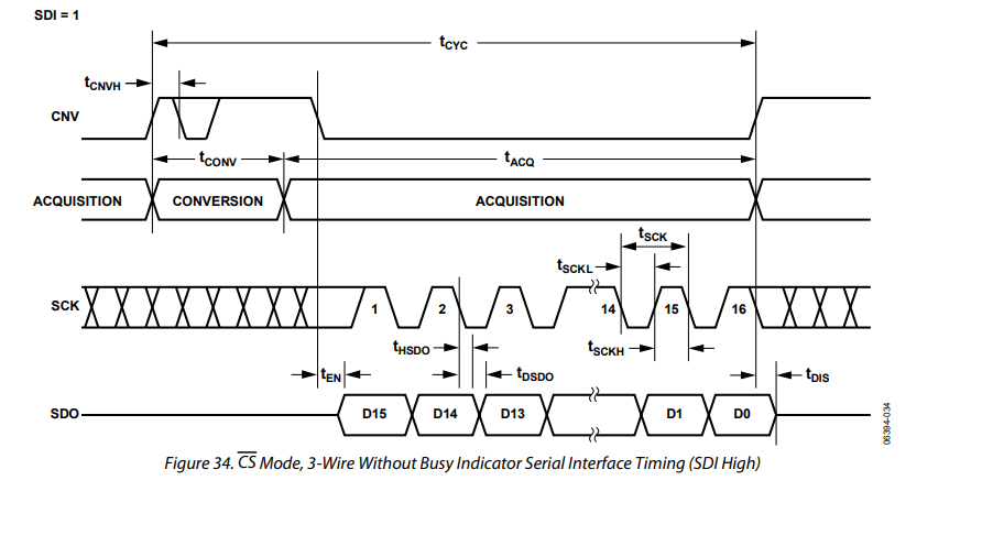
1688482717880.png


Please help me in understanding my assumptions.
1) We have TCYC=2uS=500 KHZ
2) We have TSCK=15nS=66 MHZ

So for each cycle of 66MHZ, it will sample 1 bit so in total for 16bits it will take 16*tsck=16*15=240nS?
So for 1 second, i will have 16bits/240nS=66M bits so my question is how is relation of 500KSPS?
Can you please help me understanding relations?
 
Hi,

ADC sampling rate has about nothing to do with SPI interface bit clock frequency.

If you have a bit clock frequency of 66MHz then most probably it will be discontinous. It will be quiet at least for the conversion time.

Rising edge of CONV starts a conversion
Falling edge of CONV starts the interface / data transfer

At least this is what I see from these pictures.I did not read the datasheet. (lack of time)

Klaus
 
i still try to understand,
we have have CNV signal time=2uS (Conversion time 1.6uS +Acquisition time 0.4uS=2uS), it comes to 500KHZ.

But is it means that within 2uS, we will get 500ksps? if so i think its too high?
 
Hi,

what`s the problem?
a period time of 2us equals 500 kSmpl/s
and the data transfer is done during acquisition time.

Klaus
 
Hi.

"/s" means "per second".
So a period time of 2us is basically the same as 500 kSmpl/s.

Mathematically it makes no sense to say "500 kSmpl/s within 2us".

It's like saying:
" I'm driving with the speed of 50km/h every minute"

Klaus
 
No, you are getting a sample every 2 uS.


Regards, Dana.
Hi Dana,
Thanks for your reply.
So is one sample equivalent to 16 bit? because as per timing diagram it shows Conversion phase and acquisition phase.
Please help me to understand with the help of below timing diagram
so its something,
First 2uS--> 1 Sample equivalent to 16 bit (D0-D15)
2uS to 4 uS-->2 Sample equivalent to 16 bit (D0-D15)

.... to 1second--> 500K sample equivalent to 16 bit (D0-D15)
1688712953582.png
 
The entire cycle consists of two phases, Acquisition in which the sampling capacitors
acquire their voltage from the sample, and then a Conversion phase which evaluates
the capacitors to create the 16 bit result. That is the overall cycle for one 16 bit sample,
one conversion.

1688726128993.png


The time to do the acquisition, setup the caps to get a weighted amount of charge, is minimum of
.4 uS. Then the conversion process, evaluating the caps, whose charge came from the acquisition
phase, is 1.6 uS. At the end of this you have a 16 bit result, eg in 2 uS you get a fully converted
sample out of the A/D.

So if converter running continuously in 2 uS, from the time you start the converter, you get a sample, then 2 uS later, at 4 uS from start, you get next, then 2 uS later, at 6 uS from start, you get next or
3rd 16 bit digital sample from start of converter.......rinse and repeat............ ad infinitum .......


Regards, Dana.
 
The entire cycle consists of two phases, Acquisition in which the sampling capacitors
acquire their voltage from the sample, and then a Conversion phase which evaluates
the capacitors to create the 16 bit result. That is the overall cycle for one 16 bit sample,
one conversion.

View attachment 183669

The time to do the acquisition, setup the caps to get a weighted amount of charge, is minimum of
.4 uS. Then the conversion process, evaluating the caps, whose charge came from the acquisition
phase, is 1.6 uS. At the end of this you have a 16 bit result, eg in 2 uS you get a fully converted
sample out of the A/D.

So if converter running continuously in 2 uS, from the time you start the converter, you get a sample, then 2 uS later, at 4 uS from start, you get next, then 2 uS later, at 6 uS from start, you get next or
3rd 16 bit digital sample from start of converter.......rinse and repeat............ ad infinitum .......


Regards, Dana.
Hi Dana,
Thanks for explanation, now i understood.

Last question:
We have Serial peripheral, which i believe SPI is used here.
From Timing diagram..
It has TSCK=15nS...Which means after every rise time of CLK, it will send digital data to Master with the Help of SDO.
1688727745902.png


then it will be same as SPI Protocol as per standard.
1688727911572.png

and after 16 clock cycle, we will get Hex Value of the particular data.. is it correct?
 
1688731618473.png


As you see from the timing diagram after each bit is converted, in the Conversion phase,
you can then clock out over the SPI interface. Keep in mind, read the digital interface portion
of datasheet, that the falling edge of CNV clock is the "trigger" for you to generate
the serial clock and "grab" the 16 bits from the conversion complete register while its
in the Acquisition cycle. Note the SPI clk, at 15 nS min, allows you to rapidly get the
converted sample well before next Conversion sample cycle is started. You can start the
SPI process :

1688733103318.png


So yes after 16 clocks you will have the result.

Lastly a note, since you are dealing with a 16 bit converter you need to do an error budget
thru entire signal path to see if it meets your final goal over T and V variation. This might
help - https://www.analog.com/media/en/technical-documentation/app-notes/an-931.pdf

Also this - https://www.analog.com/en/education/education-library/data-conversion-handbook.html

I would start here with your chosen Vref and its tolerances.

1688732783367.png


Regards, Dana.
 
Last edited:
Hi,

referring to your post#11:

The datasheet clearly states the the interface is SPI (compatible).

I don´t know where your pictures are from. But they don´t seem to be very reliable.
Better read SPI specification and / or documents provided by semicondutor manufacturers.

I never heared about POCI and PICO signals.
SPI signals usually are named /SS, SCK, MOSI and MISO.
Also SPI interface is MSB first whereas your pictures show LSB first.
Don´t use this as reference.

Klaus
 
Hi,

thanks for the information.

The reason for renaming the signals seems to be the confusion with human slavery.

My opinions:
* It never came to my mind to refer electric signal (names) with human slavery.
* Human slavery existed and still exists. Renaming electric signals won´t improve the situation.
* It must be bored people who decided this renaming. Renaming just pretends to do something .. but indeed avoiding these names means to avoid talking about the real problem.

--> don´t talk about slavery and slavery is gone? Close your eyes, close your ears...


Klaus
 
View attachment 183674

As you see from the timing diagram after each bit is converted, in the Conversion phase,
you can then clock out over the SPI interface. Keep in mind, read the digital interface portion
of datasheet, that the falling edge of CNV clock is the "trigger" for you to generate
the serial clock and "grab" the 16 bits from the conversion complete register while its
in the Acquisition cycle. Note the SPI clk, at 15 nS min, allows you to rapidly get the
converted sample well before next Conversion sample cycle is started. You can start the
SPI process :

View attachment 183676

So yes after 16 clocks you will have the result.

Lastly a note, since you are dealing with a 16 bit converter you need to do an error budget
thru entire signal path to see if it meets your final goal over T and V variation. This might
help - https://www.analog.com/media/en/technical-documentation/app-notes/an-931.pdf

Also this - https://www.analog.com/en/education/education-library/data-conversion-handbook.html

I would start here with your chosen Vref and its tolerances.

View attachment 183675


Regards, Dana.
Hi Dana,
I have understood till 16 Bit conversion.

1. In 2uS we will have 16 bit, so Single bit time=2uS/16=125nS.

Bit12345678910111213141516
Time (nS)125125125125125125125125125125125125125125125125

Now, i see, i have SPI Clk=15nS, So for first 8 cycle, i could read only one bit then for reading entire data i would need 16*8=128 Cycle=128*15nS=1920nS=1.92uS (~2uS)

is my understanding correct?
 
Hi,

how an ADC works:
* it acquires the analog signal
* on the rising edge of the CNV signal it starts a conversion by HOLDING the analog voltage
* during the conversion time it converts the analog signal into a 16 bit digital signal
* after conversion phase is finished you may start the interface to read out the digital conversion result
* also after conversion it starts again the acquiring phase. It may be in parallel to the active interface

--> don´t start the digital inferface before conversion is finished.

This is what the timing diagram shows.


Also
* 15 ns is the minimum value. You are free to use a higher value.
* 2 us is the minimun value. You are free to use a higher value.

Klaus
 
If you use a 15 nS clock then you get a bit each falling edge SCK, so you would
get the 16 bits in 15 nS X 16 = 240 nS. You have to complete this before the
Acquisition cycle completes indicated by a rising edge CNV signal. The CNV time
is 400 nS for a 2 uS sample rate.

Thats roughly a 66 Mhz SCK. Frankly way to high. So thats one of the reasons
I indicated you need to contact ADI to see if that register stays valid until the end
of the Conversion cycle, which would allow you to use a slower SCK. Contact ADI
and ask them if that register is double buffed, eg. an intermediate internal register
is used for the conversion process, and then when Conversion complete that reg
internally is transferred into the SPI output register, allowing you more time to get
the data, hence lower SCK. Since Conversion time is 1.6 uS that would allow you to
use a SCK of ~ (1600 nS + 240 nS) / 16 ~= 8.7 Mhz.

It might even be you can do SCK at 2 uS / 16 = 8 Mhz. Verify this with ADI. If the answer
register is simply edge triggered off a single edge in the overall conversion cycle,
eg. falling edge of CNV. - Ten of course :

1688840790483.png


Regards, Dana.
 
Last edited:
Hi Dana and KlausST,
Thanks for explanation.

What is time for single Bit in 16 bits
is it 2uS/16=125nS?
If yes, then choosing 15nS SPI Time, for at least first bit i will read only 0 or 1 and not correct data.
Let say LSB=0, LSB Time=125nS
So for first 8 cycle (15nS*8CYCLES), I will read 0 only
So, Data to the Master shall be wrong (0000 0000)

or my understanding is wrong? but i cannot imagine how it would after 16bit conversion?
 
Ignore the XXXXXXXX clocks, they are don't cares. If you let SCK run continuously,
once CNV falls low, after Ten, each falling edge for the next 16 SCKs gets the bit.
So you can use logic and a shift register to get the data. Or only burst SCK when
CNV is low. Or on receive side just use SPI capture register in the micro you are
using.

Your SCK determines bit time (bit time after Conversion is complete), and its equal
. to the period of the clock.

If you contact ADI they may have a API written you could adapt to your design.

By the way there are micros out there , ARM based, with 20 bit A/Ds on them, as
well as 12 bit SARs that can do 1 Mbps, and SPI and tons of other stuff.


Regards, Dana.
 

LaTeX Commands Quick-Menu:

Similar threads

Part and Inventory Search

Welcome to EDABoard.com

Sponsor

Back
Top