Continue to Site

Welcome to EDAboard.com

Welcome to our site! EDAboard.com is an international Electronics Discussion Forum focused on EDA software, circuits, schematics, books, theory, papers, asic, pld, 8051, DSP, Network, RF, Analog Design, PCB, Service Manuals... and a whole lot more! To participate you need to register. Registration is free. Click here to register now.

ADC Testing Issue: Can anybody help me with this?

Status
Not open for further replies.

wandola

Junior Member level 3
Joined
Jul 20, 2005
Messages
31
Helped
0
Reputation
0
Reaction score
0
Trophy points
1,286
Activity points
1,554
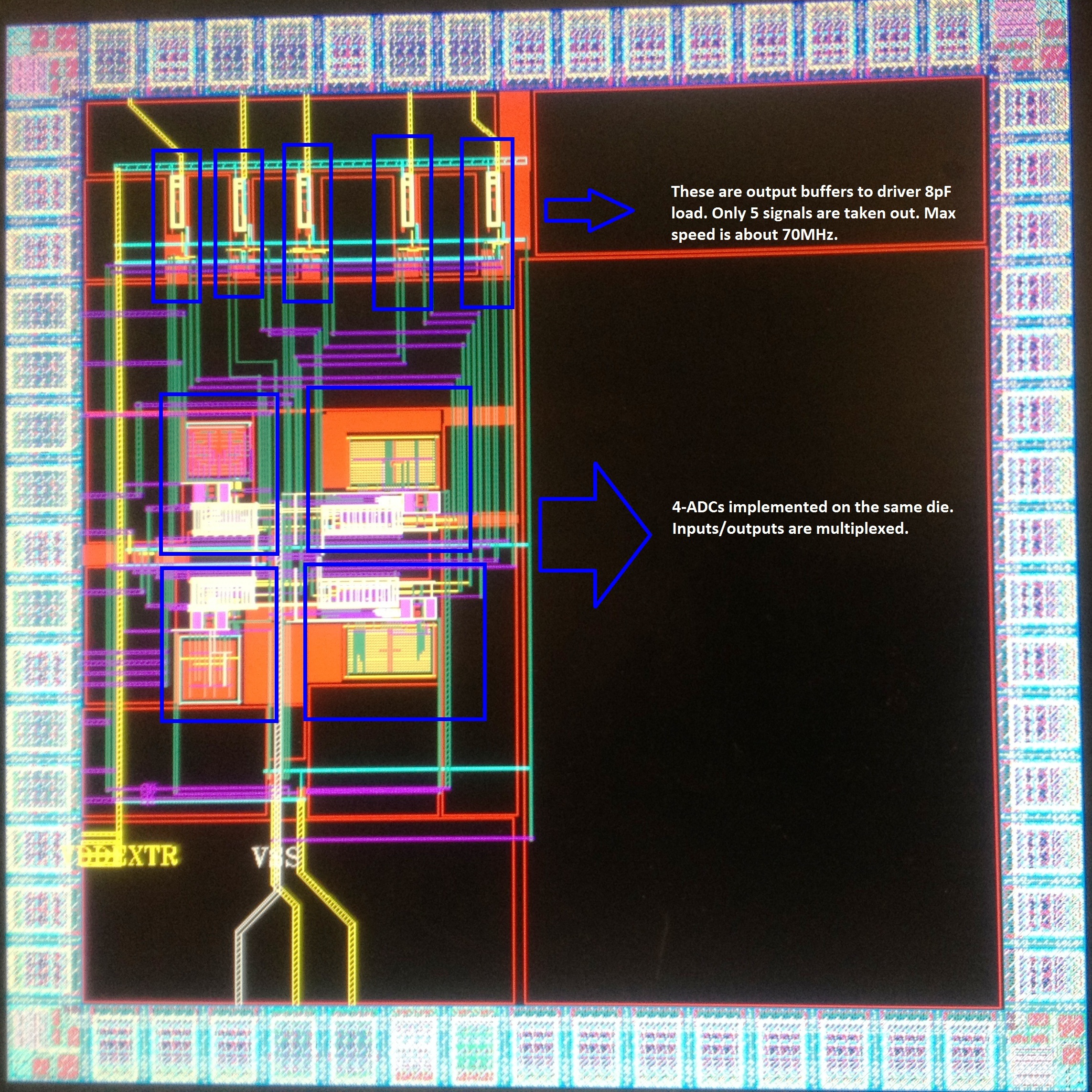
I have designed a SAR-ADC. I am doing some testing now.

I build the testing circuits. I have encountered some very funny issues which cannot be explained explicitly.

I have attached a ppt slides I sent to my boss.

The problem is that, when the output pad is loaded with something (just a wire), the ground signal becomes noisy. As a results, my other signals are all noisy, including input signals to my ADC, reference voltages, even the power supply.

--

The ADC output was designed to drive 8-pF capacitance. With the consideration of layout and parasitics, it should be able to drive at least 5pF. However, whenever the output is loaded with something, all other signals are distorted.

I don't know whether it is my ADC layout problem or the PCB problem.
 

Attachments

  • testing.pdf
    577.1 KB · Views: 138

Saying your ground signal is distorted, as shown in the second waveform is just another word for being unable to probe circuit signals correctly. I don't say it's an easy thing. We often need to use expensive active differential probes to probe high speed analog signals more or less undistorted.

The problem itself can be best described by the term "ground bounce". It's always present where fast single ended signals are driven from a chip, particularly with capacitive loads, also ADC clock inputs usually contribute to it. As a matter of fact, it's almost impossible to determine from the waveforms if the ADC operation is affected by it. It may be the case. Differential analog inputs are the most effective means against these interferences. But you have an apparently single ended reference circuit. Insufficient PSRR of the analog ADC parts may also thwart effective ADC resolution. You did't exactly tell, if you see the interferences in ADC results, so I won't guess about it now.
 

hi
i think simply add 104 (0.1)capacitor in vdd and v-in
 

It appears you are getting some parasitic oscillations in you circuit which are triggered by a load on the A/D output. Such high frequency oscillations will appear to be everywhere, even on your ground, with a standard oscilloscope connection. What is the frequency of those oscillations?

Along with added bypass capacitors, as qayyoum suggest, you might also consider adding a digital buffer circuit to the A/D output, since loading the output seems to contribute to the problem. Your cable likely adds considerably more than 5pF to the output.

Another possibility is feedback from output to input. How close are your input and output connections? Post a picture of the layout.
 

Hey crut, u can see some layout photos here.

I didn't some testing. The results are not good. I can see a lot of missing codes. I did the testing several times. Some of the missing codes are not consistently appearing but some are. So I guess the ADC performance is actually affected by the situation.

Now I really don't know how to proceed.


The existence of regular output buffers (as presumable) doesn't exclude self oscillations (= logic outputs switching arbitrarily with high frequency). An underlying problem in logic design/chip layout must be feared, however.

But the results don't yet allow to clearly decide between self oscillations or simple ground bounce. Measuring the waveform at all affected pins with a low capacitance active probe should allow to clarify what's going on.

Did you try to operate the chip with output series resistors?
 

Hey FvM, thanks for your help.

I don't understand your meaning of operating the chip with output series resistors.

Are you trying to say I can connect a resistor to the output? The output is digital output. In the measurement, I just connect the logic analyzer flying head to the output pin.

What does it mean, connecting the resistive load to the ADC?

I haven't tried it yet. I will see.
 

I said series resistor, not resistive load. E.g. 50 to 150 ohms next to the chip, it helps to isolate capacitive load. There's a certain chance, that you get at least correct digital measurements. The origin of the problem should be traced down nevertheless.
 

Status
Not open for further replies.

Similar threads

Part and Inventory Search

Welcome to EDABoard.com

Sponsor

Back
Top