Continue to Site

Welcome to EDAboard.com

Welcome to our site! EDAboard.com is an international Electronics Discussion Forum focused on EDA software, circuits, schematics, books, theory, papers, asic, pld, 8051, DSP, Network, RF, Analog Design, PCB, Service Manuals... and a whole lot more! To participate you need to register. Registration is free. Click here to register now.

[SOLVED] About NPN BJT circuit

Status
Not open for further replies.

Johnny_YU

Member level 2
Member level 2
Joined
Oct 17, 2013
Messages
45
Helped
2
Reputation
4
Reaction score
2
Trophy points
8
Visit site
Activity points
371
I have been trying to learn about how NPN BJT's work and I cant seam to understand a few things.
how to calculate Zi 、 Zo、Av (include Ro)
无标题.png
 

Johnny, it would be helpful to explain the used abbreviations/symbols (Zi, Zo, Av).
It is always good to use words instead of such symbols because there is no common (international) agreement about their meaning.
One technical answer: The design of such a transistor stage starts with your requirements (gain, quiescent current, supply voltage)
 
Hi,
Zi is input impedance
Zo is output impedance
Av is voltage gain

You can calculate Zi but for this you need to look inside the transistor i.e. you need equivalent model for BJT which includes a current source, etc.
Similarly for Zo.
And Av is very simple. It is the ratio of the output voltage to the input voltage.

First let us know, do you know how to draw an equivalent model of the NPN BJT? Please share your knowledge with us then it would be good for you to make you understand on the point of difficulty which you are having now.

Regards,
Princess.
 
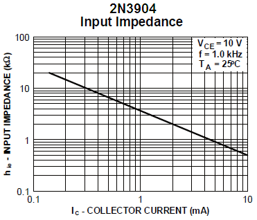
The datasheet from Fairchild for the 2N3904 NPN transistor has a graph that shows its input impedance at different collector currents. It will be the same for almost any other little NPN transistor. Their datasheet for the PNP 2N3906 transistor also has a graph of its input impedance at different collector currents.
4515854900_1401998267.png
 
I suppose, there are some other things the questioner (Johnny-YU) should know first because he is "trying to learn about how NPN BJT's work"
 
thanks for your kind advices. I wikk.

- - - Updated - - -

Hi,Eshal
thank you for your reply.
I know how to draw an equivalent model of the NPN BJT.
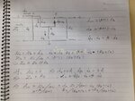
And i can work out 'input impedance(Zi)' , 'output impedance(Zo)' and 'voltage gain(Av)' without considering about the output resistor(Ro) of NPN BJT.
QQ图片20140606135114.jpg
When i consider about the Ro , i find it is not easy to work out the Zi, Zo and Av , its complex.
Do you have any suggestions
 
  • Like
Reactions: Eshal

    Eshal

    Points: 2
    Helpful Answer Positive Rating
Johnny_YU, I think, your calculations look good. I cannot see any errors.
Regarding the influence of ro=1/h22 (internal output resistance of the BJT) the approach is rather simple:
Just consider ro in parallel to Rc, that´s all (for gain and output resistance). The input resistance will be not influenced by ro.

One comment regarding the chosen circuit topology. It is not very efficient to use emitter stabilization (Re) in case of Rb current injection.
(Book from Horowitz/Hill: "Don´t do that").
It is better, to use the base voltage divider principle in conjunction with Re stabilization.
 
I have been trying to learn about how NPN BJT's work and I cant seam to understand a few things.
how to calculate Zi 、 Zo、Av (include Ro)
View attachment 106037

Actually These you are asking about are amplifier terms not related to the transistor
 
I think mnfsoft is right. You are asking amplifier Zi, Zo and Av. Not the BJT used in this amplifier. However, you did right calculations if you are asking for BJT only.

But if you are asking about the amplifier Zi, Zo and Av then you should use its AC equivalent circuit of this amplifier. It is CE amplifier. By drawing AC equivalent you can calculate first Zi and then you will go ahead.

I can show you how to do this. But you must move your steps along with me so that you could gain knowledge.
 
Hi, LvW
what's the meaning of 'emitter stabilization (Re)' ? how to explain it?
sometimes i don't know how to say some technical terms in english.
smoetimes i don't know how to explain myself clearly in english.
i think input resistance will be influence by ro, and i'm trying to prove it.
ro is tied to emitter , and Rc is tied to ground, so: 'Just consider ro in parallel to Rc' maybe not correct.

- - - Updated - - -

hi mnfsoft
you are right.
i'm talking about BJT AC Analysis and Amplification in the AC Domain.
ok,i will improve my english,thx!
 

I have been trying to learn about how NPN BJT's work and I cant seam to understand a few things.
how to calculate Zi 、 Zo、Av (include Ro)
Zi=Rin ~ hFE*(Rb+Re) ( I neglected hFE+1 as insignificant)
In 2N2907 graph since Re=0 , Rin reflect the base resistant * current gain product

Zo=Rout=Rc the collector R, since as a current source the only significant impedance is the collector resistor, But if there is a negative feedback resistor from collector to base then Rout is reduce by % amount of feedback, same as Rin. Zload must never be lower than Rc when AC coupled , otherwise it can starve collector of DC current full scale and obviously less efficient from load mismatch.

Av=Voltage gain = ratio of Rout / (Rb+Re) ....Re is external emitter R, Rb is internal base-emitter resistance, unless emitter is ;loaded with a parallel Cap then Re reduces to ESR of Cap with ReC time constant which determines low freq break point to low gain.

Consider this design of mine which has Voltage gain of 300 to 3000 with V+ from 15 to 100V and feel free to change any part value.

Sorry for my approximations. This should give you the feel of the design, you can do the math to prove if you want.
 
Last edited:
Hi, LvW
what's the meaning of 'emitter stabilization (Re)' ? how to explain it?
i think input resistance will be influence by ro, and i'm trying to prove it.
ro is tied to emitter , and Rc is tied to ground, so: 'Just consider ro in parallel to Rc' maybe not correct.

* Emitter stabilization means: Resistor Re between emitter and ground.
* If ro - in your terminology - is the output resistance of the BJT you are not correct. This resistance does not influence the input. And - yes - ro is in parallel to Rc which is connected to signal ground.

Recommendation: You should try to learn basics of transistor operation before asking questions regarding input/output resistances.
Again: Please use words instead of symbols (Zi, Zo, Av,Ro,ro).
 
I help you again. Let us first try to derive the input impedance (Zi)

I need to modify your circuit for good operation and stabilization as LvW said.

You need this design.
Capture.PNG

Is this OK uptil now?
 
Eshal and Lvw , you are right.
Using 'voltage-divider bias' is better. it can sharply reduce the effect of the current gain(hFE) which can be changed with the ambience on the quiescent operation point.
using C3 can sharply increase the voltage gain(Av).
 

i'm not trying to design a BTJ circuit
i'm trying to analyze this circuit.
here i give a re model for the common-emitter transistor configuration including effects of output resistor of the BJT(ro)
3.GIF
so it the reson why i say that the output resistor of the BTJ(ro) is not directly tied to ground. it should be tied to emitter.
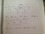
and my calculation is :
2.jpg

- - - Updated - - -

3 weeks ago, i began to read 《Electornic Devices and Circuit Theory--Ninth Edition》 written by "Robert L. Boylestad" and "Louis Nashelsky".
and today i find Eleven Edition on the net.
in chapter 5 : BJT AC Analysis ,section 5.7:CE Emitter-Bias configuration.
it shows :
4.GIF
5.GIF
6.GIF
NO derivation.
The question nagged me for days
 

Attachments

  • 1.GIF
    1.GIF
    14.7 KB · Views: 176
Last edited:

HI, LvW
I appreciate very much your help in the past few days.
I attach great importance to your comments.
Thank you!
if you are there , please read my new post and give some suggestions.
Thank you!
 

You made a mistake in your Zout calculation.
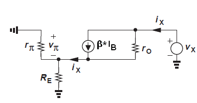
In this circuit Ib is not equal to 0A. To find Zout we "short" transistor base terminal to ground. But this "short" is only for AC signal. And this means the in real life we "short" transistor base to GND via large capacitor. So transistor is ON and still work in active region.
9076291600_1402328691.png


And to find Zout we apply Vx test voltage and we find Ix
Zout = Vin/Ix

and Ib = -Ve/RE and we also notice that RE and rpi = (β + 1)*re appear in parallel.

So

VE = Ix*RE||rpi


We also recognize that ro carries a current of Ix − β*Ib and hence sustains a voltage of (Ix − β*Ib)ro.
Then from KVL we have
Vx = Ve + (Ix − β*Ib)*ro
Vx = Ix*RE||rpi + (Ix − β*Ib)*ro

Ib we can find Ib by using current divider rule.

Ib = -Ix*RE/(RE + rpi)

So we have

Vx = Ix*RE||rpi + (Ix + β*Ix*RE/(RE + rpi))*ro

Zout = Vx/Ix = RE||rpi + ro + ro*β*RE/(RE + rpi)

Zout = Vx/Ix = ro*(1 + β*RE/(RE + rpi)) + RE||rpi

And you can try simplify this further.
 
Last edited:
You made a mistake in your Zout calculation.
In this circuit Ib is not equal to 0A. To find Zout we "short" transistor base terminal to ground. But this "short" is only for AC signal. And this means the in real life we "short" transistor base to GND via large capacitor. So transistor is ON and still work in active region.

9076291600_1402328691.png


And to find Zout we apply Vx test voltage and we find Ix
Zout = Vin/Ix

and Ib = -Ve/RE and we also notice that RE and rpi = (β + 1)*re appear in parallel.

So

VE = Ix*RE||rpi


We also recognize that ro carries a current of Ix − β*Ib and hence sustains a voltage of (Ix − β*Ib)ro.
Then from KVL we have
Vx = Ve + (Ix − β*Ib)*ro
Vx = Ix*RE||rpi + (Ix − β*Ib)*ro

Ib we can find Ib by using current divider rule.

Ib = -Ix*RE/(RE + rpi)

So we have

Vx = Ix*RE||rpi + (Ix + β*Ix*RE/(RE + rpi))*ro

Zout = Vx/Ix = RE||rpi + ro + ro*β*RE/(RE + rpi)

Zout = Vx/Ix = ro*(1 + β*RE/(RE + rpi)) + RE||rpi

And you can try simplify this further.

Great!!
Thank you so much!

- - - Updated - - -

Finally, I got it.
Haha...
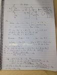
1.jpg
 

Status
Not open for further replies.

Similar threads

Part and Inventory Search

Welcome to EDABoard.com

Sponsor

Back
Top