Continue to Site
Follow along with the video below to see how to install our site as a web app on your home screen.
Note: This feature may not be available in some browsers.

I have been trying to learn about how NPN BJT's work and I cant seam to understand a few things.
how to calculate Zi 、 Zo、Av (include Ro)
View attachment 106037
I have been trying to learn about how NPN BJT's work and I cant seam to understand a few things.
how to calculate Zi 、 Zo、Av (include Ro)
Zi=Rin ~ hFE*(Rb+Re) ( I neglected hFE+1 as insignificant)
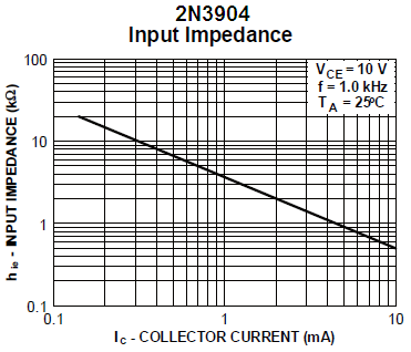
In 2N2907 graph since Re=0 , Rin reflect the base resistant * current gain product
Zo=Rout=Rc the collector R, since as a current source the only significant impedance is the collector resistor, But if there is a negative feedback resistor from collector to base then Rout is reduce by % amount of feedback, same as Rin. Zload must never be lower than Rc when AC coupled , otherwise it can starve collector of DC current full scale and obviously less efficient from load mismatch.
Av=Voltage gain = ratio of Rout / (Rb+Re) ....Re is external emitter R, Rb is internal base-emitter resistance, unless emitter is ;loaded with a parallel Cap then Re reduces to ESR of Cap with ReC time constant which determines low freq break point to low gain.
Consider this design of mine which has Voltage gain of 300 to 3000 with V+ from 15 to 100V and feel free to change any part value.
Sorry for my approximations. This should give you the feel of the design, you can do the math to prove if you want.
Hi, LvW
what's the meaning of 'emitter stabilization (Re)' ? how to explain it?
i think input resistance will be influence by ro, and i'm trying to prove it.
ro is tied to emitter , and Rc is tied to ground, so: 'Just consider ro in parallel to Rc' maybe not correct.


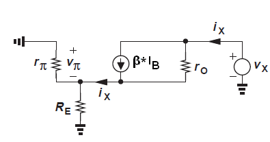
You made a mistake in your Zout calculation.
In this circuit Ib is not equal to 0A. To find Zout we "short" transistor base terminal to ground. But this "short" is only for AC signal. And this means the in real life we "short" transistor base to GND via large capacitor. So transistor is ON and still work in active region.
And to find Zout we apply Vx test voltage and we find Ix
Zout = Vin/Ix
and Ib = -Ve/RE and we also notice that RE and rpi = (β + 1)*re appear in parallel.
So
VE = Ix*RE||rpi
We also recognize that ro carries a current of Ix − β*Ib and hence sustains a voltage of (Ix − β*Ib)ro.
Then from KVL we have
Vx = Ve + (Ix − β*Ib)*ro
Vx = Ix*RE||rpi + (Ix − β*Ib)*ro
Ib we can find Ib by using current divider rule.
Ib = -Ix*RE/(RE + rpi)
So we have
Vx = Ix*RE||rpi + (Ix + β*Ix*RE/(RE + rpi))*ro
Zout = Vx/Ix = RE||rpi + ro + ro*β*RE/(RE + rpi)
Zout = Vx/Ix = ro*(1 + β*RE/(RE + rpi)) + RE||rpi
And you can try simplify this further.


")