Continue to Site

Welcome to EDAboard.com

Welcome to our site! EDAboard.com is an international Electronics Discussion Forum focused on EDA software, circuits, schematics, books, theory, papers, asic, pld, 8051, DSP, Network, RF, Analog Design, PCB, Service Manuals... and a whole lot more! To participate you need to register. Registration is free. Click here to register now.

Strange NPN and PNP pair

Joined
Mar 11, 2024
Messages
3
Helped
0
Reputation
0
Reaction score
0
Trophy points
1
Activity points
25
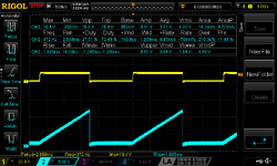
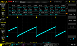
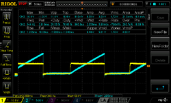
I built this 500Hz, 0-10V sawtooth wave generator i found online. I get the first block, which is just a constant current generator. But i've never seen such a transistor configuration, found in the second block. I guess it turns on the PNP when the capacitor gets to 10V, which turns on the NPN which keeps the PNP on until the capacitor reaches 0V. I'd like an explanation and some formulas, thanks


]
LBLI0F7.png
 
Where did you find this?

How can this work possibly if T1 & T2 latch On?
It looks like a failed attempt.

The left T3 is just a buffered CV from Vb R ratio and no constant current CC integration.

A current mirror is required for that.

The right side was often done by a Unijunction or a Diac. But as shown looks like a PNPN junction using the emitter input instead of the NPN base somewhat like an SCR.

A sawtooth requires a finite slew rate up and an ultrafast fast discharge or an inverted sawtooth switch. Either way you need to define specs of linearity and slew rate for each slope as this affects implementation.
I have done this for a Doppler mixer using 10 MHz sawtooth with a 100 ns cycle and a 1 ns reset for a 100:1 ratio.

What would you like to do?

kN7hK5w.jpeg


I found the reset part of the circuit interesting and i wanted to know how it works since it's pretty unconventional.
I too at first thought it was an attempt at making an scr, but while the idea is the same the SCR gate is not used, while the N-N junction is (i'm referring to the following image: https://www.google.com/url?sa=i&url=https://www.allaboutcircuits.com/textbook/semiconductors/chpt-7/silicon-controlled-rectifier-scr/&psig=AOvVaw17we91_KaeR0_Utg6gseV2&ust=1710265184729000&source=images&cd=vfe&opi=89978449&ved=0CBMQjRxqFwoTCIDQjrjg7IQDFQAAAAAdAAAAABAE
 
Last edited:
I guess it turns on the PNP when the capacitor gets to 10V, which turns on the NPN which keeps the PNP on until the capacitor reaches 0V.
Basically.
That transistor combination acts rather like an SCR.
When the capacitor voltage rises high enough to turn on as determined by the base voltage from divider resistors R4 and R5, T2 turns on, which turns on T1, discharging the capacitor.
When the capacitor voltage drops to the base-emitter voltage of T2, where T1 and T2 turn off, the cycle restarts.

Below is the LTspice sim of a similar, slightly more complex circuit:

Here the Q3 bootstrap generates a constant voltage across R4, and thus a constant-current to C1 for a linear sawtooth.

Q4 is an emitter-follower to buffer the capacitor sawtooth output.

D1 is to prevent reverse over-voltage of Q1's base-emitter junction

Note the short time that transistors Q1 and Q2 are on to discharge the capacitor (yellow traces).

The constant current of approximately 0.6V / R4 charges the capacitor up to approximately 0.6V above the divider voltage from R2 and R3, when discharge occurs, so using the capacitor equation for voltage versus charge current, you can calculate the sawtooth period.

1710179927711.png
 
The right-hand arrangement of two transistors is known as a Programmable Unijunction Transistor. It's a method to duplicate an all-in-one unijuction transistor which used to be easily available.

Circuits with explanations:

 
Thanks guys, one last thing. Does anyone know why when lowering R3 by a little changes the discharge time a lot? And why is the minimum voltage on the capacitor negative and not 0.6V like it should?
 

Attachments

  • NewFile12.png
    NewFile12.png
    44.5 KB · Views: 34
  • NewFile11.png
    NewFile11.png
    44.5 KB · Views: 33
  • NewFile10.png
    NewFile10.png
    44.8 KB · Views: 31
Last edited:
View attachment 189274

I found the reset part of the circuit interesting and i wanted to know how it works since it's pretty unconventional.
I too at first thought it was an attempt at making an scr, but while the idea is the same the SCR gate is not used, while the N-N junction is (i'm referring to the following image: https://www.google.com/url?sa=i&url=https://www.allaboutcircuits.com/textbook/semiconductors/chpt-7/silicon-controlled-rectifier-scr/&psig=AOvVaw17we91_KaeR0_Utg6gseV2&ust=1710265184729000&source=images&cd=vfe&opi=89978449&ved=0CBMQjRxqFwoTCIDQjrjg7IQDFQAAAAAdAAAAABAE
sorry but your link has no circuit like yours, but @crutschow 's has a significant difference with base drive on the left and Emitter on the right. In yours, the emitter would just be static.

With R3 on the emitter of T3 as a PNP. the base voltage controls the higher emitter voltage which controls the current of Ie & thus constant current source Ic which controls dV/dt.
 

LaTeX Commands Quick-Menu:

Part and Inventory Search

Welcome to EDABoard.com

Sponsor

Back
Top