Continue to Site

Welcome to EDAboard.com

Welcome to our site! EDAboard.com is an international Electronics Discussion Forum focused on EDA software, circuits, schematics, books, theory, papers, asic, pld, 8051, DSP, Network, RF, Analog Design, PCB, Service Manuals... and a whole lot more! To participate you need to register. Registration is free. Click here to register now.

finding Vbe in NPN Biasing

yefj

Advanced Member level 3
Joined
Sep 12, 2019
Messages
704
Helped
0
Reputation
0
Reaction score
2
Trophy points
18
Activity points
3,874
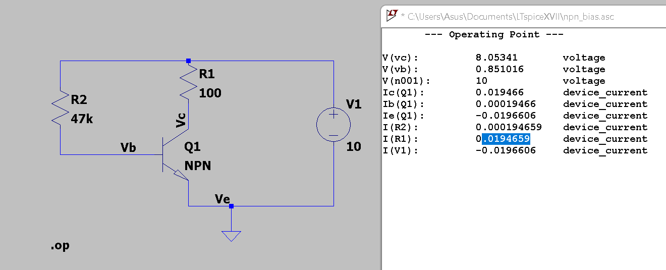
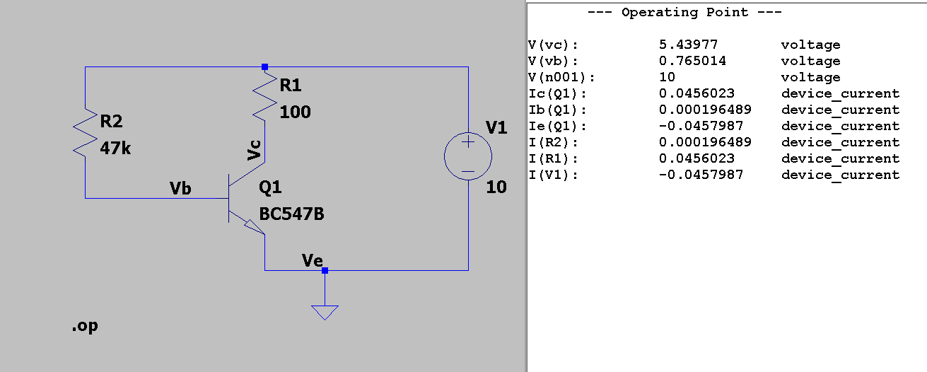
Hello,I am trying to bias BC547B NPN transistor.
We have Vcc=10V in the middle we have a voltage drop between 47k and the resistance of BE junction.
How do i know the resistance of the BE juction ?
I cant see how to get the simations result that Vb=0.76

1678138274419.png


1678138191889.png
 

betwixt

Super Moderator
Staff member
Advanced Member level 7
Joined
Jul 4, 2009
Messages
15,799
Helped
5,088
Reputation
10,201
Reaction score
4,951
Trophy points
1,393
Location
Aberdyfi, West Wales, UK
Activity points
133,788
The voltage dropped across B-E isn't a resistance, that's why it isn't easy to calculate. There is a PN junction between base and emitter so the 0.76V comes from the forward voltage dropped across it. The voltage will remain fairly constant across a wide range of base currents.

Brian.
 

KlausST

Super Moderator
Staff member
Advanced Member level 7
Joined
Apr 17, 2014
Messages
23,280
Helped
4,742
Reputation
9,505
Reaction score
5,129
Trophy points
1,393
Activity points
154,226
Hi,

What do you want to achieve with this circuit?
Switching application? Some linear regulation?

Over the thumb:
From datasheet you know V_BE is 0.55V ... 0.77V.
Start to calculate with 0.65V.
Then you can calculate I_B.
With the DC gain from the datasheet you can calculate the expected collector current.
Then you may start again by getting V_BE from datasheet, now with the use of collector current.

The problem here is that - as Brian already mentioned - the calculation is difficult.
V_BE depends on base current, collector current, temperature, production tolerances ....

So the value of the simulation ... in reality may vary a lot from transistor to transistor.

Klaus

Added: Don't use datasheets from third party. Better use datasheets directly from the manufacturer. They are most up to date, most reliable...
 

danadakk

Advanced Member level 5
Joined
Mar 26, 2018
Messages
2,296
Helped
351
Reputation
720
Reaction score
530
Trophy points
113
Activity points
10,092
Vbe :

1678145708970.png


Biasing :


Regards, Dana.
 

LvW

Advanced Member level 6
Joined
May 7, 2008
Messages
5,866
Helped
1,749
Reputation
3,504
Reaction score
1,353
Trophy points
1,393
Location
Germany
Activity points
39,880
The problem here is that - as Brian already mentioned - the calculation is difficult.
V_BE depends on base current, collector current, temperature, production tolerances ....

So the value of the simulation ... in reality may vary a lot from transistor to transistor.
And this is exactly the reason that a circuit as shown should NOT be used for amplifying purposes.
Instead, it is recommended to use DC negative feedback (emitter resistor) to make the whole circuit less sensitive to parameter tolerances of the active device (BJT).
 

LaTeX Commands Quick-Menu:

Part and Inventory Search

Welcome to EDABoard.com

Sponsor

Top