Continue to Site

Welcome to EDAboard.com

Welcome to our site! EDAboard.com is an international Electronics Discussion Forum focused on EDA software, circuits, schematics, books, theory, papers, asic, pld, 8051, DSP, Network, RF, Analog Design, PCB, Service Manuals... and a whole lot more! To participate you need to register. Registration is free. Click here to register now.

3-phase PWM Inverter with variable voltage frequency

Status
Not open for further replies.

mareast21

Newbie level 5
Joined
Jul 19, 2006
Messages
10
Helped
0
Reputation
0
Reaction score
0
Trophy points
1,281
Activity points
1,353
3 phase pwm inverter

Hi..

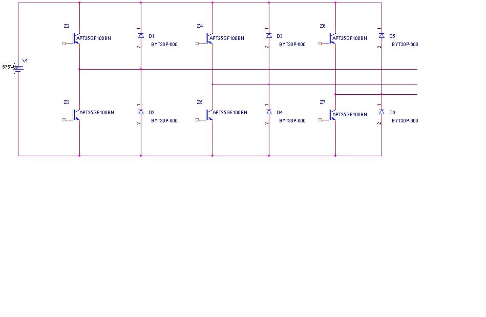
i need help here..anyone know how to design 3-phase inverter with variable voltage frequency with Pspice?i need to do simulation first.. i have the input DC supply 575V, i need output voltage variable from 50V-400V..Please help me..i have no idea to start the design..

thanks..
 

3 phase pwm

ha.. you have a difficult project ahead of you.

which version of PSpice are you using?

the hard part will be how to deal with the floating grounds of your system. each "upper" switch in your bridge has its reference to the center node between teh 2 switches. you know what i mean?

each switch needs a gate driver. each gate driver has components on it which require power and return. the return reference is floating for the upper switches. how to get PSpice to recognize this? ya.. it can be done, but it will give you some headache.

let's get started.

do you have your circuit drawn out on paper? which components you are gonig to use? start here. post your paper schematic when its ready. if you do not know which components you are using then use block diagrams for now.

Mr.Cool
 

three phase pwm inverter

thanks Mr.Cool for reply..

i'm use Orcad 9.2..


"the hard part will be how to deal with the floating grounds of your system. each "upper" switch in your bridge has its reference to the center node between teh 2 switches. you know what i mean?"

-->> i don't understand what does it mean..huhu..but i know, i need to control 6 switch..i prefer IGBT and the important things is THD < 5% for all condition and after filtering..

i will post the draft design when it ready..

thanks..
 

10 phase pwm

You didn't tell about the intended simulation level. A full circuit simulation including gate drivers and IGBTs creates a really complex circuit with possibly several 1000 internal nodes and is very time consuming. Also IGBT and MOSFET are likely to cause convergence problems in transient analysis of switching circuits.

Personally, I prefer to analyse simplified equivalent circuits representing the complete inverter power stage and control circuit. The output stage switching behaviour can be more effectively analyzed in single phase circuits, e.g. a half-bridge.

In case of equivalent circuits, the said floating nodes cause less problems in simulation than in real life. Sometimes, SPICE needs high ohmic dummy resistors to cancel special floating node problems. But these effects are not specific to power electronics and should be known by most developers.

The ideal controlled sources present in any SPICE version are effective means in creating simple isolating gate drivers or voltage and current sensors. For simulation of control circuits, it's good to have access to analog behavioral modelling, cause it considerably reduces the complexity of respective quivalent circuits.
 

design an inverter pwm driver

FvM, good info. i have simulated full bridge with IGBT and MOSFETs. it takes a fewof minutes to simulate about 30ms of data, this on a FAST quad-core computer with 4GB of ram. i find this perfectly acceptable simulation time, given the quality of the results obtained. we're not talking about matlab/simulink here, we are doing full behavioural modeling.

convergence issues can be an issue true. so take the simulation one step at a time. when you get conversence error, stop adding components and fix the problem before moving on. with this approach i have very complex models developed with no convergence issues.

finally, behavioral modeling is great for controller design, agreed. just remember that these blocks only work with their outputs referenced to system ground ("0" node). so ABM blocks can not really be used in the floating sections of your design.

Added after 2 minutes:

having said all that... lets take a step back.

mareast21, what are you interested in achieving with your simulation? basic working inverter with current control? change the voltage reference and watch your output voltage change, fully controlled. measure your output current & voltage and see FFT to asses the THD <5%?

all of these things can be done with simulink, and you will have your simulation model completed faster and more reliable.

if you want detailed simulation of component behaviours - then - you use PSpice. and maybe for just that section of the model.. then go back to simulink. for example, will your gate drive be susceptable to "miller effect" during IGBT switching? what is the power dissipation of sense resistor? under what conditions will my power supply transformer saturate? can i achieve 100% PWM with a bootstrap high-side driver (like IR2110)? these are specific questions best answered by PSpice.

so it depends on what your goals are, like FvM said.

Added after 14 minutes:

here is a PSpice gate driver IC.


you'll notice the picture is labeled as "high-side". it is infact a high-side driver, true, but.. when used in this circuit it is actually for a "low-side" switch. how do i know? because i see that the gate-drive IC is referenced to "0" ground node in PSpice. this node is ALWAYS system ground in PSpice.

also, you see only one switch (mosfet) here. you need 2 switches per "phase leg".

for IGBT, your upper switch is connected Drain to DC bus. and the upper switch's SOURCE pin is connected to the DRAIN of the lower IGBT. the lower IGBT's SOURCE pin is connected to system ground.

the midpoint between the two switches (source of upper IGBT and drain of lower IGBT) becomes "phase A" output. three such circuits is the topology of a 3-phase system.

do some research to understand what i have written here. draw your system.

Mr.Cool
 

variable voltage frequency

hi everyone..

i just draw a basic 3 phase inverter below..of course it can't be simulate..the problem now is how to control 6 IGBT...i have checked the IC driver given by Mr Cool..thanks..credit to him..but i still confusing

yeah it true..based my previous experience the convergence time become one of the issues..

i have something to ask..should i used ABM??


pspice variable pwm

the part you identified is a 1000V, 25A mosfet. not an IGBT. although PSpice shows symbol for IGBT. this is confusing.

if it is a mosfet then you do not need anti-parallel diode. the fact taht you put one in your circuit may cause problems (maybe not).

i think you should ensure that this is the part you want to use and if so, to make sure the PSpice model is represented properly.

you can work on the above in the background.

for now,
get that gate driver IC to work. show me that you can input a Vpulse and get a pulse at the output of the gate driver IC. i want to see the chip do TTL input and +15V to 0V output. preferably +15V to -5V output. make your Vpulse signal issue 20kHz (50us) , 50% dutycycle (25us period) with 50ns rise & fall time. no delay. you should see similar pulse at output of your gate drive IC.

i assume your switching frequency is going to be 20kHz.

finally.. in Pspice every component you select matters. that means, you MUST read the datasheet for every component you select. this is to ensure it fits your application & that you wire it in properly. look for design examples in the datasheet. if you read the datasheet of the switch device you selected, you would have spotted the problem so far identified. don't make this mistake twice.

Mr.Cool
 

variable inverter circuit

hmm

instead of using real components that almost cracking my head..i'm using a dummy component..just play around..the problem for the cct below is about the filtering part..
not pretty work..

well im still looking for the best n real way to solve my problem..

tq 4 ur idea..
 

3phase pwm inverter

APT25GF actually is an IGBT previously manufactured by APT, now acquired by Microsemi, I've seen the datasheet. There are newer APT25Gx devices available from Microsemi now.

A behaviour modelling circuit can be build in a similar way, but has to keep the SPICE semantics, e.g. no floating nodes. Thus the push-pull switch control doesn't work exactly as shown, but you are on a good way. The PWM generation method should basically work.

I didn't really understand, what's your filtering problem. In this design part, you have to use real circuit elements. So you either have an idea, what you want to achieve here, or you should start some more basic research.
 

3-phase inverter pspice model

i've never used ETABLE before to generate PWM.. and your connection looks odd. 2ns pulse width of V1 source? but whatever, if it works it works.

now, if your decision is to simulate a circuit using ideal components.. why are you using PSpice? the point of PSpice is that it matches well with reality. ideal components does not.

looks to me that you are not interested in actually designing anything. you just want to slap together a 3-phase inverter for the point of obtaining simulation results only. there are much easier tools to use & you definately don't need our help for this.

good luck!
Mr.Cool
 

pwm inverter using pspice

so who is interested in this design? anyone want to help out?

start with some requirements.. say, 10kW inverter for residential use.... no GRID connection (yet) ...

maybe this can be an open source project?

Mr.Cool
 

phase pwm

Hi,
I'm doing a very complex internship and I realy want your help in designing a 2 phase, sinusoidal PWM inverter , 550V , 130 Amp., Iripple=30 Amp., IGBT model no. is (FGL40N120AND), F sw.= 40 kHz, Driver model(UCC37322), Output filter (L= 300 uH, C= 940 nF), load: linear motor.
the designing of this system in based on a hard switched IGBT and I have to use a pre- PCB that used the same components with some changes because it was dealing with 25 Amp. output current.
The question is :
* could you give me the main components I have to change in order to make a suitable design without any problem in testing it?
* could you tell me which parameters I have to test in order to say that my design is working good?
Thanks in advance and I hope I can get your answer very quick because I have just 2 months to do all of this otherwise I will lose my internship:cry: !!
greetings,
Mido
 

Hi there,

I think I´m on a comparable mission...

Please have a look how far I am. It´s made with the 16.3 Version.

So far i got the PWM Logic and the Bridge. My Problems deals with the Gate Drivers. I tried to use ABM Blocks for that but theres some floating problems.

I am really new to this program, so please help!

Thanks everybody...
 

sorry, i don't have cadence installed right now.

but your problem is completely understandable to me. i solved it some time ago, and the simulation runs with realistic switching with decent speed. here i will say this up front. you must build your pspice model very slowly and compile/simulink at each step. you need to know which connection you make which craps out, super slows the simulation or has conversion issue. as soon as you see this, stop and fix your model.

now for the gate driver. you must create a power supply for the gate driver which is referenced to 0 (pspice GND). +15V and -10V with respect to ground. now put a single 1MEG resistor between ground and the +/- 15V DC supply (Vdc in PSpice). now this point, between 1 MEG resistor and +/-15V you can name that wire, say "IGBT_0" to represent the floating ground of your gate driver. for a floating gate driver driving an IGBT it is possible now. apply the +15V to the IGBT gate pin with the IGBT_0 net connected to IGBT source pin.

get it?

now.. use PSpice model E (voltage gain) to transfer your digital PWM signal - which is referenced to PSpice 0. on the primary side of "E" it is referenced to PSPICE 0 GND, but on the secondary side it is referenced to IGBT_0. so now the signal can be transfer across the border with no difficulty and fully isolate drive the IGBT.

remember what i said in the beginning..

good luck
Mr.Cool
 

HI! i need help i only need a simple PWM inverter for use in PSpice 9.2 where can i find a model or a circuit done? i doný need build it only use
 

Status
Not open for further replies.

Part and Inventory Search

Welcome to EDABoard.com

Sponsor

Back
Top