Continue to Site

Welcome to EDAboard.com

Welcome to our site! EDAboard.com is an international Electronics Discussion Forum focused on EDA software, circuits, schematics, books, theory, papers, asic, pld, 8051, DSP, Network, RF, Analog Design, PCB, Service Manuals... and a whole lot more! To participate you need to register. Registration is free. Click here to register now.

Calibre LVS nfettw error

Status
Not open for further replies.

soa

Newbie level 4
Joined
Nov 7, 2009
Messages
6
Helped
0
Reputation
0
Reaction score
0
Trophy points
1,281
Location
United States
Activity points
1,350
Dear All,

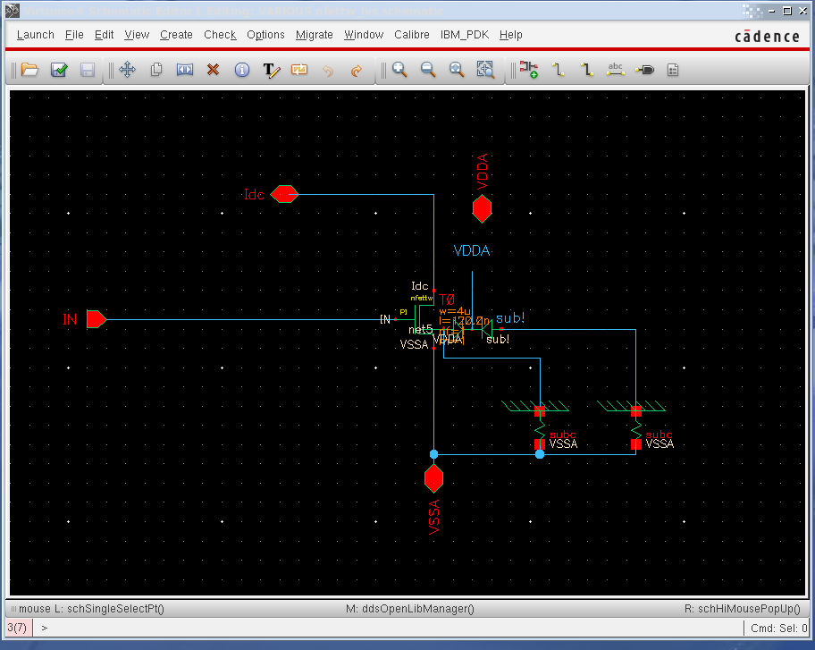
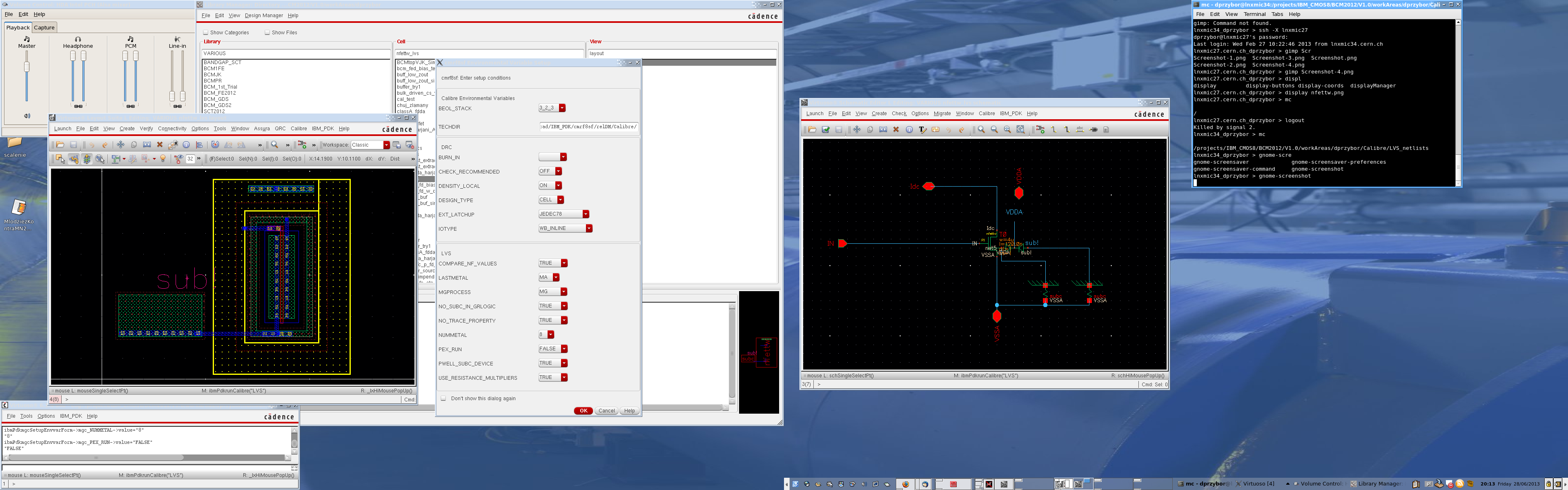
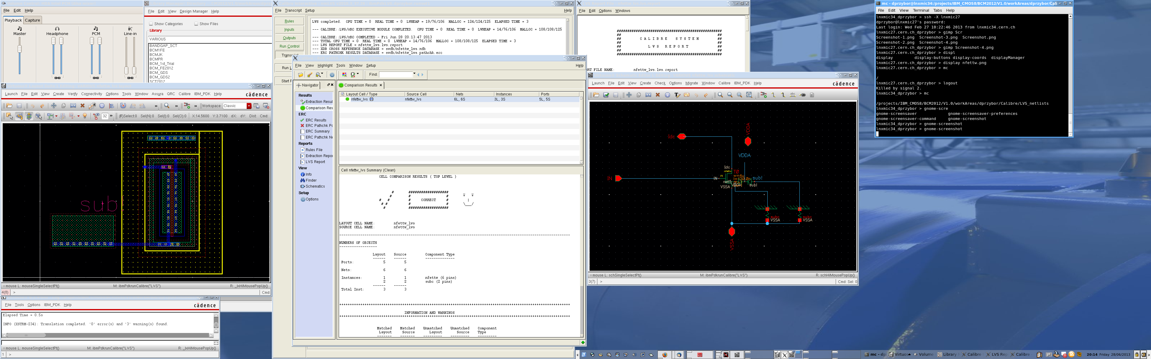
I am using IBM130nm technology,

when I want to check LVS, there is an error in mismatch between layout and schematic.

even if I use a single nfettw from standard library (cmrf8sf), the error remains the same.

the error is in number of pins: in layout the nfettw has 4 pins for fet while in the schematic the nfettw has 6 pins

I think LVS checks just 4 pins in layouts (G D S B) and separates the NW contact as new component (subc).

I appreciate if somebody can help me.

Thanks a lot
 

now i had the same problem, did you solve the problem?
 

On schematic You should have bulk and substrate (pins B and sx) connected via subc to source and ground respectively and terminal PI connected to vdd, while on the layout you need to add a contacts on inner pwell and on outer nwell.
 

yes, in schematic i used subc and also i referred to the training manual to draw the layout. I think i did it right. the extracted netlist shows nfet and 3 diodes as you can see from the attached LVS results picture. Also i attached the test schematic and layout, if someone can import this into IC61 and help me to pass LVS (if you use the same process, so i assume you have the PDK and LVS rule), that will be really appreciated!
Capture2.PNG
Capture.PNG
 

Attachments

  • nfettw_lvs.tar
    90 KB · Views: 100

I'll try to check this cell tomorrow on IBM PDK v1.8. Are You sure about using a correct calibre settings for LVS? On the first look it could be good...
In IBMCMOS8RF I using "multiple partpath" to making a well/substrate contacts and surrounded whole transistor with it.
 

I'll try to check this cell tomorrow on IBM PDK v1.8. Are You sure about using a correct calibre settings for LVS? On the first look it could be good...
In IBMCMOS8RF I using "multiple partpath" to making a well/substrate contacts and surrounded whole transistor with it.

I am using cmrf8sf v1.8, too. I am quite confident about the setup and the LVS procedure, as well as the way to draw guardrings, I did LVS and extracted simulation for the normal devices. it works well.
The only potential problem is that we are still using Calibre version 2010, it has a problem in extraction but should not affect LVS.

Thanks for your help!
 

You need add to schematic additional subc connected between nfet bulk and vssa.
Thanks!
please check the schematic i attached below
Capture_sch.PNG
But this does not change the layout extracted netlist at all. You have passed LVS with adding this with the test cell I uploaded?
 

My schematic is below:


Try to delete you lvs.netlist file, create new netlist for calibre lvs and try again.
 

Yes, I did it again. it has two errors , please check below. That's the only thing you changed to make it work?
Capture33.PNG
 

One more thing - I remove sub! pin from layout and only left a label "sub!" on sxcut layer. Below are screenshots of layout, schematic and calibre setup and result:


The netlist for calibre lvs:
* CDL Netlist updated for Extraction on: Fri Jun 28 20:12:22 CEST 2013
*.EQUIV tdndsx=diodendx
*.EQUIV ind=ind_inh
*.EQUIV inds=inds_inh
*.EQUIV indp=indp_inh
*.EQUIV bondpad=bondpad_inh
************************************************************************
* auCdl Netlist:
*
* Library Name: VARIOUS
* Top Cell Name: nfettw_lvs
* View Name: schematic
* Netlisted on: Jun 28 20:11:46 2013
************************************************************************

.INCLUDE /vlsicad/micsoft/IBM_CMOS8_V1.8_DM_vcad/IBM_PDK/cmrf8sf/V1.8.0.4DM/cdslib/cmrf8sf/subcircuit.cdl
*.EQUATION
*.SCALE MICRON
*.MEGA
.PARAM

*.GLOBAL sub!

*.PIN sub!

************************************************************************
* Library Name: VARIOUS
* Cell Name: nfettw_lvs
* View Name: schematic
************************************************************************

.SUBCKT nfettw_lvs IN Idc VDDA VSSA
*.PININFO IN:I Idc:B VDDA:B VSSA:B
XT0 Idc IN VSSA net5 VDDA sub! nfettw m=1 l=120.0n w=4u nf=1 par=1 ngcon=2
+ mSwitch=0 idg=0 t3well=0 psp=0
XI3 VSSA net5 subc
XI0 VSSA sub! subc
.ENDS
 
  • Like
Reactions: prcken

    prcken

    Points: 2
    Helpful Answer Positive Rating
I still have 2 discrepancies.
Capture3.PNG
the netlist for LVS is below
netlist.PNG

Can you send the worked cell file to me? I just want to check whether my Calibre is too old caused this problem.

BTW, which Calibre version you are using?
 
Last edited:

I'm using Calibre .v2010.3_37.26.
This cell matched in lvs for me.
 

Attachments

  • nfettw_lvs.tar
    90 KB · Views: 77

Thanks, I used your cell and tried again, still has two discrepancies :sad:.
my Calibre is v2010.2_38.23. I think I setup it correct and used the right rules (IBM_PDK/cmrf8sf/V1.8.0.4DM/Calibre/LVS/cmrf8sf.lvs.cal). I have no idea what is the problem now. maybe have to try to update the Calibre

BTW, have you tried to run with my file without modifying? did it pass?
 
Last edited:

Remove you old netlist.lvs file, generate a new one and try again. Sometimes calibre don't overwrite a lvs netlist file.

//edit. You first attachment containing schematic cell and layout didn't match.
 

yes, i did remove and generate a new one. :sad:

still the problem is "nfet" in the extracted netlist instead of "nfettw", this kills me

Capture4.PNG
 
Last edited:

Thanks, Dominik,
I was waiting update the Calibre, after updating, i tried but couldn't pass LVS, so that I go back to check the setup you posted again. My bad, I didn't notice and didn't follow your setup the PEX_RUN switch set to be "FALSE". It passed LVS after setting PEX_RUN switch to be "FALSE" for both older and newer versions of Calibre.
Then I read the cmrf8sf.CalibreLVS.ref_notes, at page 9, it states " In order to have clean LVS comparison, subcircuit definition for the triple well FETs should be included in subcircuit.cdl file for schematic netlist and the PEX_RUN switch should be set to FALSE. If the PEX_RUN switch is set to TRUE the triple well FETs will be extracted as four terminal devices with three parasitic diodes representing the pn junctions."
 
Last edited:

Dominik,
do you know the IBM 130nm model includes the cap corner or not? it seems there is no corner considered for cap from the simulation.
thanks
 

I don't know. I know only that models for rf transistors including more things than "normal" ones.
 

Status
Not open for further replies.

Part and Inventory Search

Welcome to EDABoard.com

Sponsor

Back
Top