Continue to Site

Welcome to EDAboard.com

Welcome to our site! EDAboard.com is an international Electronics Discussion Forum focused on EDA software, circuits, schematics, books, theory, papers, asic, pld, 8051, DSP, Network, RF, Analog Design, PCB, Service Manuals... and a whole lot more! To participate you need to register. Registration is free. Click here to register now.

Calibre LVS nfettw error

Status
Not open for further replies.
I don't know. I know only that models for rf transistors including more things than "normal" ones.

i have found out that the resistor and capacitor skew is setting by changing the values of the "cor_res" and "cor_cap" switches in the design.scs file.
 

Hi Dominik,

Do you have any suggestion to pass multiple nfettw devices? Again, I had trouble in passing LVS. Can you help to have a try to see what's the problem? I uploaded the file below.
Thanks!
 

Attachments

  • TIA_tst.gz
    43.7 KB · Views: 61

I don't know. I know only that models for rf transistors including more things than "normal" ones.

Hi Dominik,
Any tricks for layout more than one nfettw devices? I still got stuck at here :( 
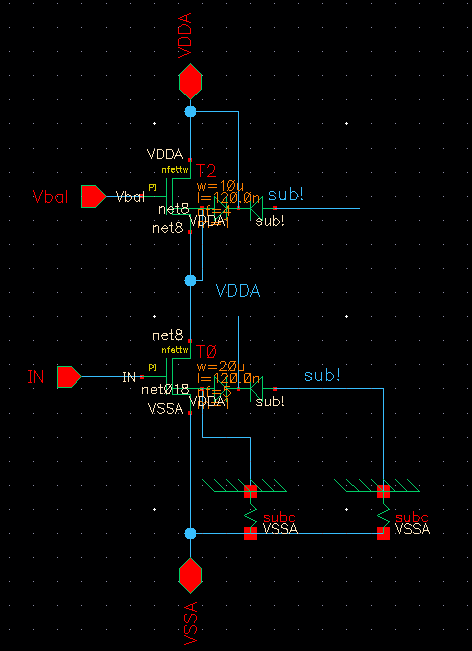
I can only pass the single nfettw device
Help!
 

If You have triple-well nfet with source connected to other net than gnd!, You should connect bulk with source while PI on vdd! and sx on sub!.
 

If You have triple-well nfet with source connected to other net than gnd!, You should connect bulk with source while PI on vdd! and sx on sub!.

Hi Dominik,
good point! Indeed I didn't connect like that.
I've changed the upper nfettw device bulk to source connection, but still LVS has problem. It's weird in the LVS results to show that the source of layout of the upper device connected to VDDA.
I have uploaded the pictures below for you to check, can you have a guess what may cause the problem? can I send you the schematic and layout files?
Thanks!
 

If You have triple-well nfet with source connected to other net than gnd!, You should connect bulk with source while PI on vdd! and sx on sub!.

Hi Dominik,
If you have time, can you please import the attached test file to Cadence and help to check what's wrong with it? what you said about the triple-well nfet the source connect to bulk is correct, but i don't think not doing this will cause the LVS problem.
I think the problem is still the subc symbol.
Really appreciate if you can help. Thanks in advance!
 

Attachments

  • nfettw_2device.gz
    22.2 KB · Views: 59

Some years ago I heard about t-shirt with printed ibm130nm subc cell ;-)

You need to add third subc between source and bulk of T2 transistor.
 

Attachments

  • nfettw_2device.tgz
    22.9 KB · Views: 64
  • Like
Reactions: prcken

    prcken

    Points: 2
    Helpful Answer Positive Rating
Some years ago I heard about t-shirt with printed ibm130nm subc cell ;-)

You need to add third subc between source and bulk of T2 transistor.

Hi Dominik,
I am excited, this problem bothered me for a long time. Thank you very much, I have tried to add another subc anywhere but never thought about add between source and bulk. now I will try with more than 2 devices including the dummy devices layout work, and see if any other problem will come out.
 

now I know the tricks and can pass LVS with many nfettw devices :) your information is very helpful, thanks
 

Dominik, have you ever used this IBM 130nm process to generate 3.3V RC clamp ESD protection circuits? I can pass LVS with 1.2V devices, but for 3.3V devices, it has some problem.
1. if i don't choose T3 layer, DRC has problem
2. if I choose T3 layer, the LVS has problem.
Thanks!
 

Hi Dominik,
I have the nfettw device LVS again, but this time is IBM8HP process.
I thought I follow the CMRF8 process should pass LVS, but it turns out not.
layout_Schmeatic.png
LVS_report.PNG
Can you take a look?
Thanks!
 

I don't see a contacts to inside p-well, which should be source. IMO the sub! net should be only on substrate contact outside the fet.
 

sorry, i just saw your reply.
I tied several ways before i made this post, now i removed the sub! on the p+ inside the Nwell, i did add contact and v1 to n3 net. still the same LVS error
Capture.PNG
 

Status
Not open for further replies.

Part and Inventory Search

Welcome to EDABoard.com

Sponsor

Back
Top