Continue to Site

Welcome to EDAboard.com

Welcome to our site! EDAboard.com is an international Electronics Discussion Forum focused on EDA software, circuits, schematics, books, theory, papers, asic, pld, 8051, DSP, Network, RF, Analog Design, PCB, Service Manuals... and a whole lot more! To participate you need to register. Registration is free. Click here to register now.

complementary input folded cascode opam

Status
Not open for further replies.

Junus2012

Advanced Member level 5
Joined
Jan 9, 2012
Messages
1,552
Helped
47
Reputation
98
Reaction score
53
Trophy points
1,328
Location
Italy
Activity points
15,235
dear friends

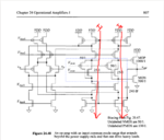
I am designing a folded cascode opam just like in the attached image,

I have question about this circuit, in typical folded cascode opamp we have current source and current mirror, but in this configuration we only have mirrors, one at the top and one at the bottom,

so how the currents at the output stage is summed, if we know that one of the current is comming from the differential tail current, the other one from where??

I am just thinking that the other current is from the floating current transistors but I am not sure, and if it is true the what are the rules for designing this circuit.

let us assume that I will use a differential tail current = 50 uA.

I would appreciate any kind of help
Thank you in advance
 

Thank you

I forgot the image,, here it is
 

Attachments

  • Screenshot from 2018-12-06 17-45-49.png
    Screenshot from 2018-12-06 17-45-49.png
    136.8 KB · Views: 189

I recommend you a book where the why is exactly explained, I don't remember exactly:
Operational Amplifiers - Theory and Design
Authors: Huijsing, Johan
(https://www.springer.com/gp/book/9789400793002)

But you can create rail2rail in/out version of this amplifier for example with PMOS current mirror at the top, and NMOS current sources at the bottom, sometimes that has other advantage, if I remember well the DC offset of above version is worse, but I am not sure.
 
thank you fran for your help but this circuit is should i work with and i am not fully understanding it
 

frankrose is right: "Try SCE to AUX." /John Aaron/. It really worked, then ;-)

Your circuit question about the function of this high swing cascode current source was also explained in one of Johan Huijsing's original papers: "Low-Power Low-Voltage VLSI Operational Amplifier Cells" by Johan H. Huijsing, Ron Hogervorst, and Klaas-Jan de Langen in IEEE Trans. Circuits Syst. I: FUNDAMENTAL THEORY AND APPLICATIONS, VOL. 42, NO. 11, NOVEMBER 1995, which you can download freely.

See pp. 848 ff. Fig. 24 & 25, and the text explanation thereof.
 
I'm happy you, erikl also like this quote. And good article by the way. Have a good evening! :)
 

Thank you Erikl for your reply

I am pleased that you still active in this forum, you helped me a lot many years ago when i was doing my thesis

back to the circuit, I took a look on the circuit of Huijsing, it is the same explained by Holberg, you can see that he put current source at the bottom of the output stage and current mirror at the top, this procedure is actually followed by most of the references,

The one I should follow is the one from Jakob which I attached his image,

since there is no current source neither at bottom or the top, does it mean that the output current is set by the floating current sources (from Jakob circuit)

I must use the floating current source because I need to use the output class AB buffer stage

let us suppose that my differential tail current is 50uA to make it reference point for your suggestions

Thank you very much in advance
 

... there is no current source neither at bottom or the top, does it mean that the output current is set by the floating current sources (from Jakob circuit)

No, there are current sources at the bottom and also at the top: these are Cascode or High-Swing current sources - like in this image:
Cascode_or_High-Swing_Current-Source.png ... controlled by Vbias3 and Vbias2 .
 
Hello Erikl,

Thank you for your reply

Actually I see that Vbias3 and Vbias4 are not used to source or sink currents, these voltages are used to bias the wide swing mirror for each the top and down,,

even if you come to your circuit you can see that there is current source symbol Iref1 0 30 uA, and M4 transistor output voltage is only to fix the M5 to minimum sat region...


I mean if in your circuit there is a symbol of current source, how the case with the output stage of my circuit.

thank you and sorry to make it long
 

Actually I see that Vbias3 and Vbias4 are not used to source or sink currents, these voltages are used to bias the wide swing mirror for each the top and down,,

Hi Junus,
I think there is a misunderstanding: the bias voltages for the wide swing mirrors are Vbias3 and Vbias2, not Vbias4.


even if you come to your circuit you can see that there is current source symbol Iref1 0 30 uA, and M4 transistor output voltage is only to fix the M5 to minimum sat region...
I mean if in your circuit there is a symbol of current source,
This above figure, i.e. the current source + its left MOSFET (M4) as a voltage source was just meant as an example for the generation of the control voltage of a wide swing mirror. You have to consider the base connection between M4 and M5 as the bias voltage for the wide swing mirror, i.e. Vbias3 respectively Vbias2 .

how the case with the output stage of my circuit.
Vpcas and Vncas are the control voltages of the floating current sources - the right one of them controls the quiescent current through the output stage.
 
Thank you erikel for your reply

now you came to my point,

yes in these two days i read the article you gave to me, he is saying that this floating current source will set the output stage current,

the only difference now, some of the references says we set the current at the output stage equal to the one of the differential tail current (in my circuit diagram I1=I2=differential tail current),
some of them says to the half of it. and I am confused by it.

I would also ask you please about the slew rate, which formula govern this topology.

still I have couple of doubts but I will discuss about it after clearing this issue
 

the only difference now, some of the references says we set the current at the output stage equal to the one of the differential tail current (in my circuit diagram I1=I2=differential tail current),
some of them says to the half of it. and I am confused by it.

Both indications are not correct: your I1 & I2 source the operation currents for the n-channel input stage, respectively sink the operation currents of the p-channel input stage, that's why they (I1 & I2) must be bigger than these operation currents of the differential input stage, at least by a factor of 2 , better 3 .


I would also ask you please about the slew rate, which formula govern this topology.

The slew rate δVout/δt essentially is given by the max. current of the output stage Imax, and its load capacitance CL: δVout/δt = Imax / CL .
 

Status
Not open for further replies.

Part and Inventory Search

Welcome to EDABoard.com

Sponsor

Back
Top