Continue to Site

Welcome to EDAboard.com

Welcome to our site! EDAboard.com is an international Electronics Discussion Forum focused on EDA software, circuits, schematics, books, theory, papers, asic, pld, 8051, DSP, Network, RF, Analog Design, PCB, Service Manuals... and a whole lot more! To participate you need to register. Registration is free. Click here to register now.

Diff amp with very low input voltage noise?

Status
Not open for further replies.

mtwieg

Advanced Member level 6
Joined
Jan 20, 2011
Messages
3,835
Helped
1,310
Reputation
2,626
Reaction score
1,405
Trophy points
1,393
Activity points
29,370
I'm trying to design a fully differential IF amplifier in 0.5um On semi process, and its input referred noise voltage is going to be critical in the system's overall performance. The source impedance is low, in the range of 50-1000 ohms, so to keep NF<3dB I'll need vg on the order of 1-2nV/√Hz. The operating frequency range is around 200kHz-2MHz, so flicker noise isn't a huge issue, and power consumption isn't critical either.

This is my first time doing a CMOS LNA at low frequencies, so I'm trying to get a feel for how to approach this. Most of the literature I'm finding either deals with RF frequencies, or very high source impedances and therefore higher tolerable vg noise. From my shallow understanding of device noise, my goal should just to boost the gm of my input devices as much as possible. I've run simulations on some simple circuits and I can get around 3nV/√Hz by just using huge devices and hitting them with lots of bias current (like w/l=800/3um and Ids=1ma). Simulations indicate that my overall noise is dominated by the input diff pair. Switching between nmos or pmos devices doesn't seem to make a huge difference, for some reason.

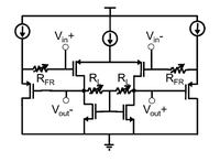
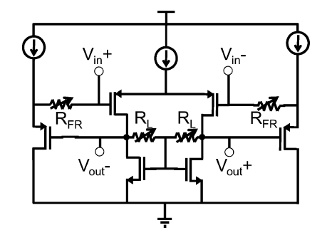
Here's a schematic of the simple circuit I'm simulating. RL is for CMFB while Rfr is for tuning gain.


I actually wouldn't mind just scaling size and gm up even higher, but my space is somewhat limited, and I'm wondering if there's anything more clever than just throwing power and size at the problem.

Also I know that BJTs would probably be ideal for this, but I don't think they are available for my process, at least certainly not in my NCSU model kit.
 
Last edited:

You can get the lower noises for input fets by biasing them in weak inversion. For 2 nV/√Hz, gm of input fets should be at level of 3 mS what is possible for 150 µA of drain current (inversion coefficient around 0.2-0.4). So assumming current gain factor for nmos as 100 µA/V² your W/L shouldbe around 2250. Of course You should to minimize gm of current sources loading input transistors.
 

Thanks for the reply Dominik. I'm not experienced in weak inversion design, but I've read quite a bit. I did a quick simulation with your parameters and yes I can get <2nV (per device) with those parameters, but that transistor ratio is enormous, even with L=Lmin. And I have to set L much higher to keep the noise corner below 200kHz, so I end up with very infeasible transistor sizes. Also I'm concerned that linearity and dynamic range will be greatly degraded weak inversion operation. If power consumption were critical then I would probably not have a choice other than weak/moderate inversion, but thankfully that's not the case.

I'm basing my work off a publication where the original authors used a 65nm process, and claimed to achieve 400pV/√Hz. They don't specify what mode their devices are biased in, but they use that same basic circuit. Is such a low noise number just a perk of the 65nm process? I don't have a spice model for 65nm to compare with.
 

Input transistor of one of my preamplifier has 4400µm/0.35µm so W/L=2250 is not enormous :)

BTW. Using minimum L is not recommended for low noise design (additional excess noise caused by not-equillibrium carriers transport in fets with L<100nm and velocity saturation). In addition even in weak inversion, short channel effects degrades fet transconductance.

Could you post title/authors of this publication?
 

Here's the publication in question:
https://ieeexplore.ieee.org/stamp/stamp.jsp?arnumber=1046463

The LNA itself is not really the meat of their research, so it's only mentioned briefly, even though it's pretty critical to overall performance.

If I had to guess, I'd estimate I have about 100,000um^2 for the LNAs (four of them). As you point out, using short channels isn't wise. My simulations suggest that L=3um gets the noise corner sufficiently low. But then if I use W/L=1000 then I'm just not going to have the space.

But I wanted to clarify, when they say they get 400pV/√Hz, is that feasible mainly because of the process they're using? Their die photo doesn't give a good sense of scale for the size of their LNAs, but it doesn't seem like they're so massive that they can achieve that based on size alone. Surely having a thinner tox and K' helps as well?
 
Last edited:

I asked for this paper about LNA in 65nm. If You are using 0.5µm process You don't need to worry about excess short channel noise (when I wrote previous post I suggest this 65nm process)
 

Is such a low noise number just a perk of the 65nm process?

Following Binkley's book "Tradeoffs and Optimization in Analog CMOS Design", which comprehensively deals with MOSFET noise and LNAs (in 0.5 .. 0.18µm processes), this is not the case. At table 3.30 he presents a totally process size-independent convenient expression for the gate-referred thermal-noise voltage PSD (Power Spectral Density) of a MOSFET: View attachment Binkley__Gate-referred_thermal-noise_voltage_PSD.pdf.

n is the substrate factor, changing from 1.3 in weak inversion (WI) to 1.4 in strong inversion (SI), and Γ is the thermal-noise factor for operation in saturation, which changes from 0.5 in WI to 0.65 in SI. All other dependency is only on temperature and gm.


I don't have a spice model for 65nm to compare with.
For comparison purpose you could use the PTM models.
 

Following Binkley's book "Tradeoffs and Optimization in Analog CMOS Design", which comprehensively deals with MOSFET noise and LNAs (in 0.5 .. 0.18µm processes), this is not the case. At table 3.30 he presents a totally process size-independent convenient expression for the gate-referred thermal-noise voltage PSD (Power Spectral Density) of a MOSFET: View attachment 114747.
Odd, I really want to read this pdf, but for some reason it's causing adobe to crash repeatedly...

n is the substrate factor, changing from 1.3 in weak inversion (WI) to 1.4 in strong inversion (SI), and Γ is the thermal-noise factor for operation in saturation, which changes from 0.5 in WI to 0.65 in SI. All other dependency is only on temperature and gm.
Right, and gm is what benefits from a higher K' at 65nm, correct?
 

Quite well description about noise analysis and optimization is presented in this thesis in chapter 3. In fact it is done for electronics for radiation detectors not for LNA but You should understand the basis.

The benefits in smaller technologies are from current gain factor (higher gm for the same dimensions and current), but what I mentioned earlier, short channel devices in decananometer processes suffer for excess noise caused by SCE.
 

Odd, I really want to read this pdf, but for some reason it's causing adobe to crash repeatedly...
Sorry, I can open the re-downloaded file without problem. I'll present it here as a PNG image: Binkley__Gate-referred_thermal-noise_voltage_PSD.png.

... gm is what benefits from a higher K' at 65nm, correct?
Not necessarily: In that "convenient equation", K' is already hidden in the gm/Id expression.

And not to forget: those sub-micron processes already show non-negligible gate current (tunnel mechanism), which additionally contribute noise.
 

Status
Not open for further replies.

Part and Inventory Search

Welcome to EDABoard.com

Sponsor

Back
Top