SACHIN C
Full Member level 2
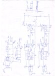
Dear All,
Pls guide me to get thru the problem related to MOSFET Switching.
Mosfet using K62j60W(Max. 600V/61.8A)
Driver used is TD350E which is able to source 0.75A other then 25c.
But,Mosfet needs 1.5A @ full load.Since presently am testing for at no load,the gate waveform shows On/OFF behaviour near falling edge.
Push -Pull Transiter used are TIP122 & TIP127 with base resistor as 33K(as HFE is 3500) & collector resistor used is 33ohms.
Mosfet Gate resistor used is 10ohm,gate to source resistor used is 10Kohm.
Supply used for Collector & Driver is 15V made from 7815(for no load testing as it is not able to deliver current for full load which is 1.5A in our case).
Thanks & waiting for valuable help.....")
Pls guide me to get thru the problem related to MOSFET Switching.
Mosfet using K62j60W(Max. 600V/61.8A)
Driver used is TD350E which is able to source 0.75A other then 25c.
But,Mosfet needs 1.5A @ full load.Since presently am testing for at no load,the gate waveform shows On/OFF behaviour near falling edge.
Push -Pull Transiter used are TIP122 & TIP127 with base resistor as 33K(as HFE is 3500) & collector resistor used is 33ohms.
Mosfet Gate resistor used is 10ohm,gate to source resistor used is 10Kohm.
Supply used for Collector & Driver is 15V made from 7815(for no load testing as it is not able to deliver current for full load which is 1.5A in our case).
Thanks & waiting for valuable help.....
Attachments
Last edited: