Continue to Site

Welcome to EDAboard.com

Welcome to our site! EDAboard.com is an international Electronics Discussion Forum focused on EDA software, circuits, schematics, books, theory, papers, asic, pld, 8051, DSP, Network, RF, Analog Design, PCB, Service Manuals... and a whole lot more! To participate you need to register. Registration is free. Click here to register now.

CMOS dc -dc convertor design M.E project

Status
Not open for further replies.
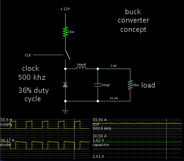
someone please help me with this ckt. This is a synchronous buck converter. The first pdf(up1) is my circuit diagram
When i do not connect the filter and take the output directly at the source of the top switch i get the graphs as in the second pdf(up3) with an average voltage of more than 3V.
But when i connect the filter across it ,the average voltage is not even 1V ,3rd pdf(up2). Whats the problem with this
My specifications used are
Vin=12v, Vout=1.6V ,D=0.133,Fs=500K,Iload=130A,Iripple=39A(30% of Iload),Vripple=10mV.
Please help , I am stuck because of this.
 

Attachments

  • up1.pdf
    13.2 KB · Views: 63
  • up3.pdf
    57.5 KB · Views: 74
  • up2.pdf
    16.7 KB · Views: 61

Your load R1 is labelled '0.0123'. That is as good as a short circuit.

My simulation shows that for 1.6V output, your load can be .038 ohm, and you'll get 41.8 A. This is with 0.2 ohm 'On' resistance in the switches.

If you want to succeed at powering a load of .0123 ohm, you need practically zero resistance in your switching devices.

It is a lot to ask for.


But my original problem still remains.I changed the load accordingly and recalculated inductance and capacitance. But i still get the same problem. when i connect the filter across the switches the average voltage drops below 1 and so i dont get 1.6V output, i get output in 600 millivolts
Help me in that please.
 

Your smoothing capacitor is labelled 300 uF. At 500 kHz you could get by with a much lower value. Maybe 30 uF. Just to see if the scope shows a change in output volt level. (You can adjust the uF higher if you want less ripple).
 
Your smoothing capacitor is labelled 300 uF. At 500 kHz you could get by with a much lower value. Maybe 30 uF. Just to see if the scope shows a change in output volt level. (You can adjust the uF higher if you want less ripple).

I checked by changing the capacitance, there is no change in output level. Changing the Capacitance is just changing the ripple. Then i tried changing the inductor value for the same capacitance. So then i found the output changed. I became some 0.9V (more then the previous 600mv). I think i have got the values absolutely wrong due to some mistake.
 
Last edited:

Your smoothing capacitor is labelled 300 uF. At 500 kHz you could get by with a much lower value. Maybe 30 uF. Just to see if the scope shows a change in output volt level. (You can adjust the uF higher if you want less ripple).

Got my design working.Downloaded the buck calculator from TI which gave me the inductor and capacitor values. Now towards a two phase buck
Thanks
 

input voltage 12V,Output voltage 2V,maximum dynamic output voltage error 100mv , with 5% peak regulation.
What does this 5% peak regulation mean(Von=+-0.05)
 

Your smoothing capacitor is labelled 300 uF. At 500 kHz you could get by with a much lower value. Maybe 30 uF. Just to see if the scope shows a change in output volt level. (You can adjust the uF higher if you want less ripple).


I have noticed there the output volatge of the buck depends on the load current. A buck designed for 5V output(vin 12,Fs=400Khz) and 2A load current works properly with l=12.12uH and C=19.5uF. However its output volatge starts to drop when the load current is increased for the same design. I think this was the problem happening to my previous design. So what changes have to be made for the design to compenstate for the load change and bring the the output proper.
My design for 32.5A current still dosent give 1.6V output(i get 1.5V and load current of 28A)
My design specs are for single phase
Vin=12V.....Vout=1.6V....D=0.133.......Fs=500K......Iload=32.5A........current_ripple=20%.....Voltage_ripple=20%...L=0.748uH....C=101.56uF
Please help

Yes, when you increase the load it decreases the volt level. The way to bring it back up is to increase the duty cycle (switch-On time).

If the switch is a transistor you might also have to boost its bias, in order to admit more current during 'On' time.

Screenshot of my simulation using your latest values:


I had to increase the duty cycle to about 3X your figure of D=0.133.

The 10 milli-ohm resistor represents some amount of resistance in the power loop. It is unrealistically low so as to get 32 A going through the converter, but we can do that because this is just a theoretical simulation.

How do you determine how much to increase the duty cycle ?
what is the relation to justify the increase ?
 

How do you determine how much to increase the duty cycle ?
what is the relation to justify the increase ?

The longer time the switch is 'On', the greater the current through the coil.

To achieve a given volt level on the load, you need to keep the switch on long enough for current to build.

The greater the resistance in the power loop, the longer you need to extend switch-On time.

If there could be zero resistance in the power loop, your duty cycle of .133 could be sufficient. However it is more realistic to expect there to be 1/10 ohm or more in the power loop. Even that much is a lot more than your load of .05 ohm. Hence it will require a longer duty cycle, in order to let coil current reach 34 A. As it turns out, the converter must operate in continuous conduction mode, at 10% above and below an average, to power the load. It is close to the upper limit of performance in a buck converter.

This is not impossible to achieve with real hardware. But consider that a flyback converter could more easily be made to perform to your specs. A flyback would take 12V at average 4.3 A (theoretically), chop it, run the pulses through a transformer, and give you 1.6V at 32 A.
 

This is a subckt of a power inductor

B82471A1104K000 SMT Power Inductor 6.1 x 6 x 4.9 (mm) Standard performance (100 uH +-10%)
*
.subckt B82471A1104K000 A1 A2 PARAMS:
+ ls11=100.7287u rs11=469.2m cp11=3.2701p rp11=112.4184k
+ lwira1=24.9900n lwa1=749.7411n rwa1=166.5808m lwb1=293.8053n
+ rwb1=1.6338 kw1a1=0.9999
X1 A1 A2 B8247X_BASE1 PARAMS: ls11_a={ls11}
+ rs11_a={rs11} cp11_a={cp11} rp11_a={rp11}
+ lwira1_a={lwira1} lwa1_a={lwa1} rwa1_a={rwa1}
+ lwb1_a={lwb1} rwb1_a={rwb1} kw1a1_a={kw1a1}
.ENDS

can someone tell me what do these parameters mean and where they are in the datasheet.I had checked but could not relate all parameters.I know there is a inductance, series DCR, a parallel capacitor and again a parallel resistor, but here i see more of them which i cant understand what they mean
 

Multiphase buck converter

Hello, i had already started on the buck converter a long back ago and was working towards improving the transient response of the multiphase buck.I have chosen the synchronous buck topology with specs(vin=12 Vout=1.2 Fs=500K Iout=40Amps) .I have found factors affecting it
1) circuit parameters- mainly ESR ,ESL of capacitor ,DCR of inductor
2) Feedback system
basically i have read only about the circuit parameters till now. And many people have already optimized these parameters for improved response. Can someone tell me some parameter that i can research on and will help me improve the transient response
Please help
 

i want a control loop based on inductor ripple. I want to implement the feedback loop with digital control(a microcontroller). The currents will be very high(50A) with frequency of 500K. Is it possible to be done ? and please provide some help if possible.
 

Please someone tell me whats the problem with this ckt.Why am i getting convergence error for this
First pdf is my ckt and second is the netlist
Convergence problems occur only when i connect the LT1394
Please help
 

Attachments

  • SCHEMATIC1 _ PAGE101.pdf
    16.1 KB · Views: 68
  • par.out.pdf
    23 KB · Views: 68

Please someone tell me whats the problem with this ckt.Why am i getting convergence error for this
First pdf is my ckt and second is the netlist
Convergence problems occur only when i connect the LT1394

U2 is getting positive supply at both pins. As for U1A, it's hard to tell.

Current will flow upward through M1/D1. Hence it makes a difference how you orient these components. In this development stage it may be easier to use only a diode pointing upward.
 

U2 is getting positive supply at both pins. As for U1A, it's hard to tell.

Current will flow upward through M1/D1. Hence it makes a difference how you orient these components. In this development stage it may be easier to use only a diode pointing upward.

Here i have put my new schematic and i know when i get the convergence error. Here LM393 is a comparator. As you can see it is working standalone in the ckt.It gives proper pwm with the dc voltage connected, but when i connect out(as labelled in the schematic) to Inverting(as labelled in the schematic) i get the error.All the ckts standalone work proper. I get the error voltage and also the pwm is coming. But when i connect them together it gives convergence error.I am not at that level to decrypt that error by myself.I think my buck converter stage is proper if i am not mistaken.Also using only a diode is not making any difference. So please if you can pinpoint something to get rid of the error.
 

Attachments

  • SSbuck.pdf
    16.1 KB · Views: 65

Often convergence errors occur when I have 3-terminal devices, and I power them from one supply voltage, yet drive the base/gate from a different voltage. In real life it is not necessarily an error. But the simulator gets confused.

In particular, your buck converter has a 12V supply. The mosfet gates are driven by 20V. There's a chance this causes the error. It would be easier if the simulator would tell us, wouldn't it?

Another possibility: mosfet M2 is N-type. Its gate is referenced to the source terminal. For it to turn on, it needs to see a definite lower volt level at the source terminal. However there are components intervening in the path to ground.

Furthermore when it turns on, it conducts 12V to the node below it, and the node goes to almost 12V. To solve this with real hardware we drive the gate with 20V... But how the simulator interprets it, only the simulator knows.

It may help if you use a P-mos for the high side.

i got the convergence problem solved. Pspice has a auto converge option that solved it.Thanks very much
 

Status
Not open for further replies.

Part and Inventory Search

Welcome to EDABoard.com

Sponsor

Back
Top