Continue to Site

Welcome to EDAboard.com

Welcome to our site! EDAboard.com is an international Electronics Discussion Forum focused on EDA software, circuits, schematics, books, theory, papers, asic, pld, 8051, DSP, Network, RF, Analog Design, PCB, Service Manuals... and a whole lot more! To participate you need to register. Registration is free. Click here to register now.

Transistor for microwave amplifier

Status
Not open for further replies.
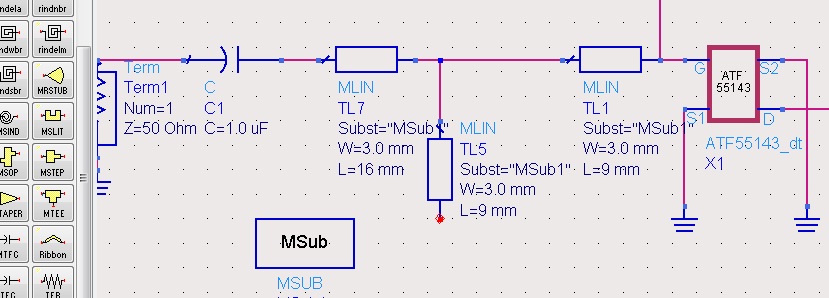
anyone ? I have completely no idea how to continue it with ADS.
 

The line software is used to calculate the line width, look at the picture you attached, the 50 ohm line width is shown at the width tab. and the length is 90 deg .
 

Tony_lth, that was my setting. I follow books. 90deg and 50 ohms.
I dont know how to set the Transistor voltage. You know ? I cannot simulate the circuit.

---------- Post added at 11:32 ---------- Previous post was at 11:08 ----------

Tony_lth, that was my setting. I follow books. 90deg and 50 ohms.
I dont know how to set the Transistor voltage. You know ? I cannot simulate the circuit.
 

1st set Vb, then say Ve=Vb-0.7V, then Ie=Ve/Re, say Vce=1V, Ic=(Vc-Vce-Ve)/Rc. Simulate it, then you can get voltage and current.
 

hmm , i am using Low Noise Enhancement Mode Pseudomorphic HEMT. so I dont know how to set the Vds, Ids

Recently I spoke to a Master student. He just roughly told me about the transistor amplifier design. I cannot ask him more, since he dont want to talk with me.

From the short conversation, I know I need to design the DC biasing network, stand alone S2P (with ADS) and lastly matching network( microstrip line).

Firstly, the dc biasing network. I know there are two types, Active and Passive. I cant tell the difference between them. I was trying to do with Active.

I found a few circuits. I dont know how to design it with the information from the transistor datasheet. There are a few inductors and capacitors which I dont know how to calculate the value. To be true, I have no idea how to start at all.......

I am not lazy or waiting for people to feed me... I hope someone can give me some idea how to continue (start) my project. I am desperate with my school lecturer. I have been reading some thesis and books, but still, I dont understand them.
 
Last edited:

I have follow the LNA design by BOY.
I was stuck at here. I cannot get the desired Ids. I have no idea how to modify it until I get the Vds and Ids. Anyone can guide me ?
 

Attachments

  • Biasing.rar
    5.3 KB · Views: 60

you can skip that if you use S-params.
 

skip it ? I need the biasing network for my hardware fabrication, so i still need to do this, right ?
Last time, I was using S param to simulate and (add Lumped components and check on the Smith Chart) match the transistor, then create a new S2P file.
After that I will use the new S2P file to continue my project. This is what the Master student told me. Althought I not really understand him, but i still give it a try.

Now I am trying the LNA tutorial by BOY, still dont understand it.
If you dont mind, please advice me.
Thank you. Really appreciate your helps.
 

The tuning DC bias is independent with S-params. According to the datasheet, You can set, say Vgs=-0.3V, and Vds=2V. The 1st thing When you start to test, is tune the Idc. You can use a potentiometer to adjust the Vgs to get the requirement Idc.
 
Oh , I see. I might have confused you. At first, I was refering LNA_design by BOY. I found I not understand the steps, I changed my mind when I read about the S2P simulation.
I have using S2P to do all the matching. But then I stucked again. I have been asking my project supervisor about it, he have no idea at all.
That is why I have more reading and understand a bit on the LNA_design by BOY. So now I am refering his tutorial as my guideline.
I have to fabricate the hardware out, that why I still need to learn how to design the Biasing network. I now still like a "new newbie" on microwave amplifier design.
I understand what tony_lth talking about, later I try to do it.

I now going to class.

By the way, Thank you.
 

I have followed the tutorial and done with my amplifier design.
S_param at 2.5Ghz:
S11 = -23.940 dB
S12 = -23.365 dB
S21 = 17.438 dB
S22 = -6.786 dB
K is 1.055 at 2.5Ghz.
This only for the stability factor and gain.

I was stucked at the NF circle.
From the page 32(the LNA tutorial), I cannot set the load and source impedance. I am using ADS 2008. I dont know how to set the setting.

Another problem, I am using ATF 55143, how do I set the biasing circuit at 2V , 10mA?
I followed the steps from the tutorial, I can able to get a 4v, 40mA.

I dont understand why he using 4v , 40mA. How to determine the 40mA? From the beginning, it stated as 4v, 20mA (page 8)

Please advice me.
Thank you.
 

You can change the bias resistor to get 2V/10mA.
And 1st you should carefully read the guide, step by step to follow it. Then do your design.
 
I have redesign it with 2V ,10mA. It is working.
 

Hi all,

Can anyone help me on this?
Page 23 from the LNA_tutorial, I dont know how this formula works.
 
Last edited:

Do you mean the mark1 "m1"? You need to set the 1st mark.

---------- Post added at 23:19 ---------- Previous post was at 23:18 ----------

Or do you mean the trans line length?
 

Sorry, I think I should ask 1 question at one time.

Here is my problem: From page 23, I noticed there are a formula of converting a small inductor value into stripline.
I have try to calculate the Length ( in mm ) , same with the tutorial setting, but I cannot get it.
How do he manage to get the length in 0.6 mm, width in 0.5mm? I mean the 0.5 x 0.6 mm microstrip line represent the 0.3nH inductor.
 
Last edited:

If I guess your question right, you can simulate it in AWR or ADS.
 

Hmm, I dont know how to do it. I know how to use the Line_cal inside the ADS, but I dont know how to implement it into the line_cal, since it is involve the inductance.
 

I have another problem.

I have one 50ohm transmission line, open stub matching microstrip lines.
How do I combine them together when I want to fabricate them into PCB.
 

There is a "junction" palette in AWR, that have a "Tee" for combing 3 lines , and "Cross" for combining 4 lines. The same is in ADS.
 

Status
Not open for further replies.

Part and Inventory Search

Welcome to EDABoard.com

Sponsor

Back
Top