Continue to Site

Welcome to EDAboard.com

Welcome to our site! EDAboard.com is an international Electronics Discussion Forum focused on EDA software, circuits, schematics, books, theory, papers, asic, pld, 8051, DSP, Network, RF, Analog Design, PCB, Service Manuals... and a whole lot more! To participate you need to register. Registration is free. Click here to register now.

[SOLVED] Question with Fiducial points

Status
Not open for further replies.

mmitchell

Advanced Member level 4
Joined
Dec 3, 2011
Messages
107
Helped
0
Reputation
0
Reaction score
0
Trophy points
1,296
Activity points
2,203
Hi,


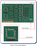
  1. On many boards there are fiducial points. I googled this, and the purpose seems basically reference/marking points to help machine vision system to do registration.
  2. Fiducial point.png
  3. However, fiducial point concept also exist the alignment of different PCB layers. The following screenshot is from page 14 of Kraig Mitzner’s book Complete PCB Design Using OrCAD Capture and PCB Edito:
  4. Fiducial point_layer.png

I have three questions:

For (1), if the board is an experiment board would have its BGA and other fine pitch components registered by human inspection before soldering, are fiducial points still required?
For (2), I have only seen Mitzner’s book mentioned this. Is it a must with today’s board manufacturing technology?

And how can fiducial points for purposes (1) and (2) be differentiated? I assume each fiducial point can actually serve both (1) and (2)?


Matt
 

I havn't used local fidusials for years (12+), but always use three fids on a board layed out to form a right angle triangle.
For most modern day pick and place machines local fids are not realy required these days as they use cameras to locate and orientate devices on the fly using the footprints. I do my own panelisation and use panel fiducials, which I can reference each individual PCB pattern to. Dont worry about lamination fids, the PCB manufacturer will sort these.
SMEMA guide on fids:
http://www.dynamixtechnology.com/docs/smema3.1.pdf
Also ref IPC-222x standards

When you do your pick and place file you add the global fids at the top of the file so that the pick and place patern for that board can be registered with the panel.
 
marce,

I could generally get the idea and will consult assembly houses on this. But if the board is going to be soldered manually for testing, does it mean I don't need to place any fiducial this time?

Many latest electronic products have very high placement density, for example Apple's iPhone. I google its image. Can you see any fiducial on the board?


Matt
 

It may be hand soldered at the prototype stage and fiducials will not be required, however what to do if the board works first time?
Will you redo the board, costing you more money just to put fiducials on?

If you have the opportunity then it is best to put them on at the start.
 
They will have fiducials on the board, it is the reference point for pick and place, and it also references the root pattern to tha manufacturered panel, that may have many PCB images.
As to your second point, yes I can see fids on all the SMD layers, and trust me they will be there.
Agree with Mattylad, also it should be standard practice when doing SMD designs. A lot of company's have the fiducials as part of the default schematic so that they are not forgotten. Again always adding them is best practice and should be the default for ANY SMD design.
These days with more modern pick and place machines you can get away with smaller fids than the SMEMA reccomended.
For your elcuidation here is a sample of a generic pick and place file, showing the fids at the begining, and more importantly a FID being at 0,0 (ie the origin for the pick and place file and thus the design pattern:

"Refdes,part No,x,y,theta,side"
FID1,,0.000,0.000,,Top
FID1D,,7.000,-8.250,,Top
FID2,,0.000,72.750,,Top
FID3,,95.750,72.750,,Top
T1,Z1000102,75.850,71.200,270.000,Top
R81,Z1000102,94.650,50.700,180.000,Top
R80,Z1000102,91.000,50.700,0.000,Top
U11,Z1000102,63.600,72.725,90.000,Top
D17,Z1000102,16.300,53.600,0.000,Top
R73,Z1000102,91.000,52.500,0.000,Top
 
Mattylad,

Thanks for the suggestion, I will keep fiducial points.

marce,

Thanks for the pick and place files. Now I can fully understand it.


Matt
 

One more point to remember about fiducials when you have a square or rectangular PCB is not to have them symmetrical placed.
The board could be feed backwards into the p&p machine and the camera would not pick up on the error.
 
Also try and ensure that any SMT components are within the boundary created by them.

Having components in both positive and negative coordinates of a fiducial can cause some placement
machine programmers to have to do more maths when programming the machine (depending upon the machine).
 
loosemose and Mattlad,

I got it, thanks for reminding.

Matt
 

Loosemoose, :-D I tend to put a big arrow on the panels to help production plave the panels the right way down the line. I have had a production line once use only two of the 3 fids (that were perfectly diaganel) and they did try realy hard to build the board rotated, whoops. On the otherside, I have had subcontract boards with no fids!!!!
As I do panelise I like to use the panel border to provide assembly depts' with information such as direction, bar code and any other info that might help achieve 98% throughput.
 
Ditto the above, I have put arrows, board no, stock code etc in the borders so that no matter what longest side you look at (there are 4) you can read this information.
Also consider tooling holes for test jigs, bad board markings and keep everything clear of the edge of the board where the machinery may grab the edge.
 
Status
Not open for further replies.

Part and Inventory Search

Welcome to EDABoard.com

Sponsor

Back
Top