yefj
Advanced Member level 4
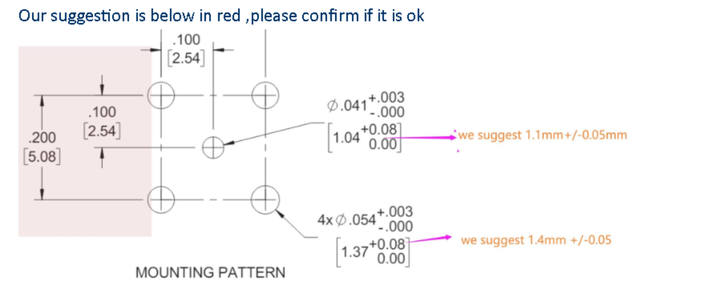
Hello , I am trying to define a hole and ORING according to the data sheet and recommendation of the manufacturer bellow.
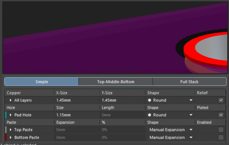
I see the pad hole option is the stack below where is the option for pad diameters?
i have defined the pad according to the data sheet , Hole=1.15 ALL_layers=1.45(I cant see the option for pad diameter)?
What should i do when defining top paste and solder mask for my pad, what diameter should i put for them?
Thanks.

