Continue to Site

Welcome to EDAboard.com

Welcome to our site! EDAboard.com is an international Electronics Discussion Forum focused on EDA software, circuits, schematics, books, theory, papers, asic, pld, 8051, DSP, Network, RF, Analog Design, PCB, Service Manuals... and a whole lot more! To participate you need to register. Registration is free. Click here to register now.

Simple folded cascode design problem

Status
Not open for further replies.

viperpaki007

Full Member level 5
Joined
Jul 2, 2008
Messages
270
Helped
11
Reputation
22
Reaction score
8
Trophy points
1,298
Location
Finland
Activity points
3,395
Hi,

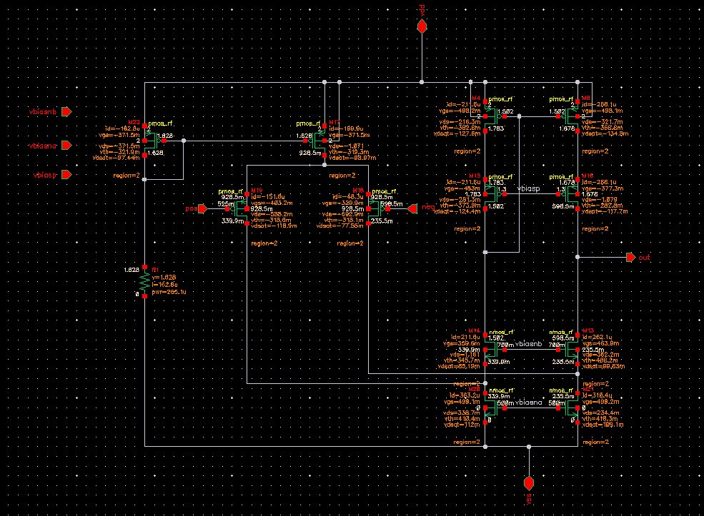
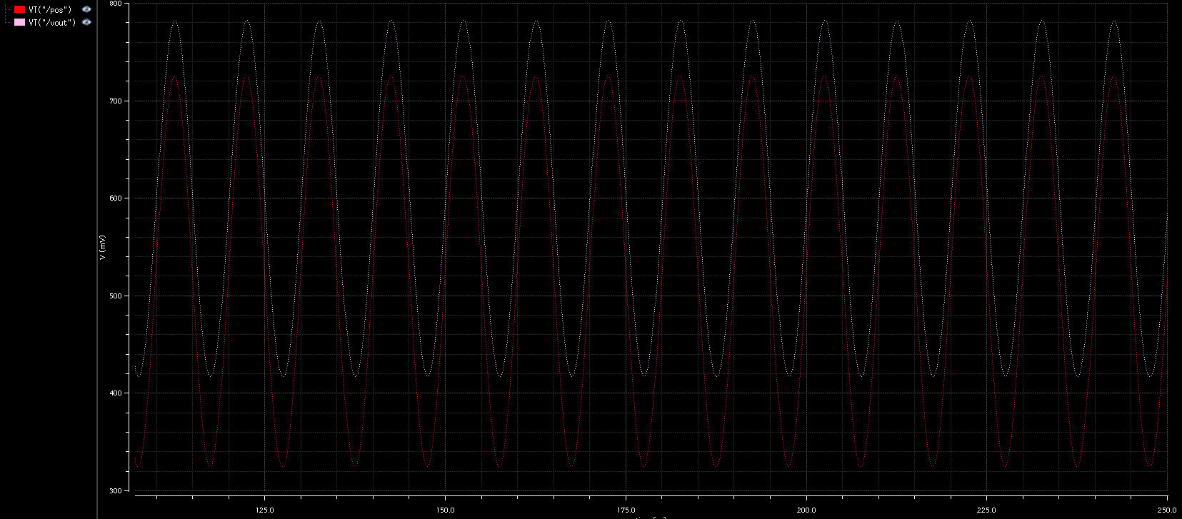
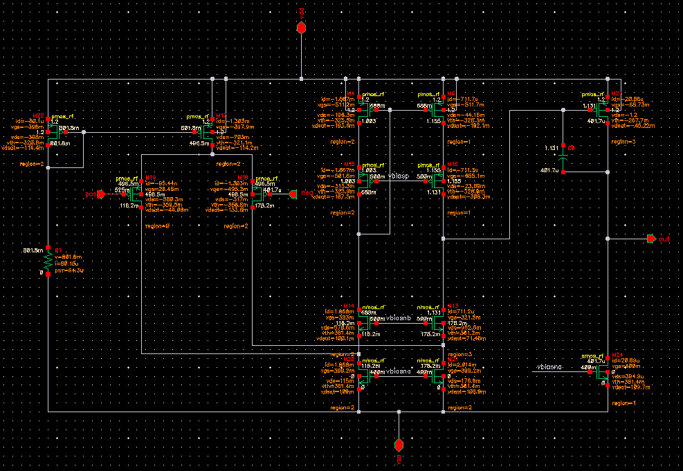
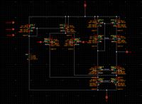
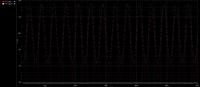
I have made a simple folded cascode structure (Circuit diagram attached). All the transistors are working in saturation. However, i have a small problem. When i put the opamp in unity buffer configuration, the output voltage is at at higher dc-offset. I don't know how to make the dc-offsets and input and output equal. Can anybody help. Simulation results are attached.


Did you set the DC levels of the op-amp... correctly?
 

folded cascode OPA is not suitable for unity buffer,you can get the reason in Razavi<Design of analog CMOS intergrated circuit>. but if you really want to use folded cascode as unity buffer,you can try to change the w/l to make the out DC voltage near to your wanted voltage(the input voltage of unity buffer),this means the input voltage should have a narrow range.
 
Hi,

If u want this amplifier to work as a buffer, you can connect a CS stage , which gives the output you need,,,... surely this will help you to get a buffer configuration,


Otherwise Try a Rail to Rail op-amp with CS gain stage...

Thanks...
 
Hi,

I thought that telescopic cascode amplifier is not suitable for unity buffer configuration rather than folded cascode. Can you tell me any rail to rail opamp configuration which i can use for high voltage swing unity buffer design
 

Hi,

I thought that telescopic cascode amplifier is not suitable for unity buffer configuration rather than folded cascode. Can you tell me any rail to rail opamp configuration which i can use for high voltage swing unity buffer design

hi,

You can simply use this configuration as a rail to rail op-amp by adding an "nmos" differential pair and give the output to a single stage CS amplifier with pmos load....

You can get good and accurate result..

Any help just let me know... i will help..

Tahnks
 

Hi Kenambo,

How can i change the dc-levels of the output because as far as i know, i can only change the W/L ratio of the output to control overdrive voltages of output transistor. However, i need to control VDS of output transistors so that at quiescent operating point VDS becomes equal to common mode input voltage. Any suggestions how to control VDS?

Did you set the DC levels of the op-amp... correctly?
 

Hi Kenambo,

How can i change the dc-levels of the output because as far as i know, i can only change the W/L ratio of the output to control overdrive voltages of output transistor. However, i need to control VDS of output transistors so that at quiescent operating point VDS becomes equal to common mode input voltage. Any suggestions how to control VDS?

Hi viper,

Actually it is not good to set output voltage in this cascode pair configuration.... Because it makes it difficult to set vds of the botom N mos pairs... So quiescent operating points are difficult to achieve....

So just add an Cs stage after the cascode output.... and Make the CS Stage's outpet as accurate DC level.... This will help i think,,

And,, By using CS configuration... at the output... you can get good output swings......

Thanks.. hope this will work for you...
 
Hi Kenambo,

How i can change the output dc-level of CS stage without affecting the overdrive voltage of transistor. By changing W/L ratio of output stage, i can adjust the VDS voltage of output stage and hence the output quiscent point. However, it will also change the overdrive voltage of output transistor. I want to keep the overdrive voltage of output transistor to be 0.1V and not more than that.

Hi viper,

Actually it is not good to set output voltage in this cascode pair configuration.... Because it makes it difficult to set vds of the botom N mos pairs... So quiescent operating points are difficult to achieve....

So just add an Cs stage after the cascode output.... and Make the CS Stage's outpet as accurate DC level.... This will help i think,,

And,, By using CS configuration... at the output... you can get good output swings......

Thanks.. hope this will work for you...

- - - Updated - - -

Hi Kenambo,

I added CS stage at the output of folded_cascode structure and tuned the output dc-voltage in open loop to be equal to input common mode level of 525mV. All the transistors were operating in saturation. However, as soon as i connected the opamp in unity buffer configuration, everything went wrong. Transistors start operating in triode and cuttoff regions and there is no output at all.. I am attaching the figure...


I still see your pos & neg terminal are the same even after adding the 2nd stage. Was the connection corrected in simulation?
 

Hi Viper,
One query : The bulk of NMOS (M14,M13) is connected to their sources. Is it Okay?
 

I did not get what you mean by "you have same pos and negative terminals"


I still see your pos & neg terminal are the same even after adding the 2nd stage. Was the connection corrected in simulation?

- - - Updated - - -

All transistor bulks are connected to sources

Hi Viper,
One query : The bulk of NMOS (M14,M13) is connected to their sources. Is it Okay?
 

Hi Viper,
Usually Nmos are fabricated over wafer (P-Substrate) directly So their bulks are shorted and connected to most Negative or Zero supply. So NMOS bulk in cascode position need to be connected to VSS. But this is not the case for PMOS as they are fabricated in NWell and their bulk can be connected locally to their sources.

What Yuvan was pointing : After adding one more stage, you are adding 180deg phase shift (CS stage). and if you are not changing the input terminals and connect output to -ve terminal then it becomes +ve feedback system and you will not get correct results.
 
Thankyou skamthey , changing pos and neg terminals really worked..:)
 

play with the sizes of bottom most nmos so that the vdsat increases to 200mV & increase the voltage "vbiasnb" such that the vds of bottom transistors is >350mV.. this will solve your problem even for the single stage.. make sure you are not using your input common mode below 200mV
 

Status
Not open for further replies.

Part and Inventory Search

Welcome to EDABoard.com

Sponsor

Back
Top