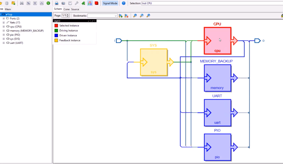
FGPA, ASIC or SoC designers use a variety of HDL's (hardware description languages) including Verilog, VHDL or SystemVerilog which can complicate visualization of complex designs. This is particularly the case when having to analyze designs from other engineers in your team and trying to figure out the interconnects which are causing issues.
Many digital design engineers wish to be able to get an automatic graphical representation of a specific verilog/VHDL module hierarchy showing which blocks are connected to which other blocks. You can now quickly import large design files and generate circuit schematics to understand functionality, drill down hierarchically and trace logic through your design quickly. See how in this 3 min video .
You can also view other RTL schematic extraction videos here that require no additional coding.