aj_silverthunder
Full Member level 3
guys please please solve this thing........
here i have made two different circuits.....but i have a big big doubt that which is correct and which is wrong...
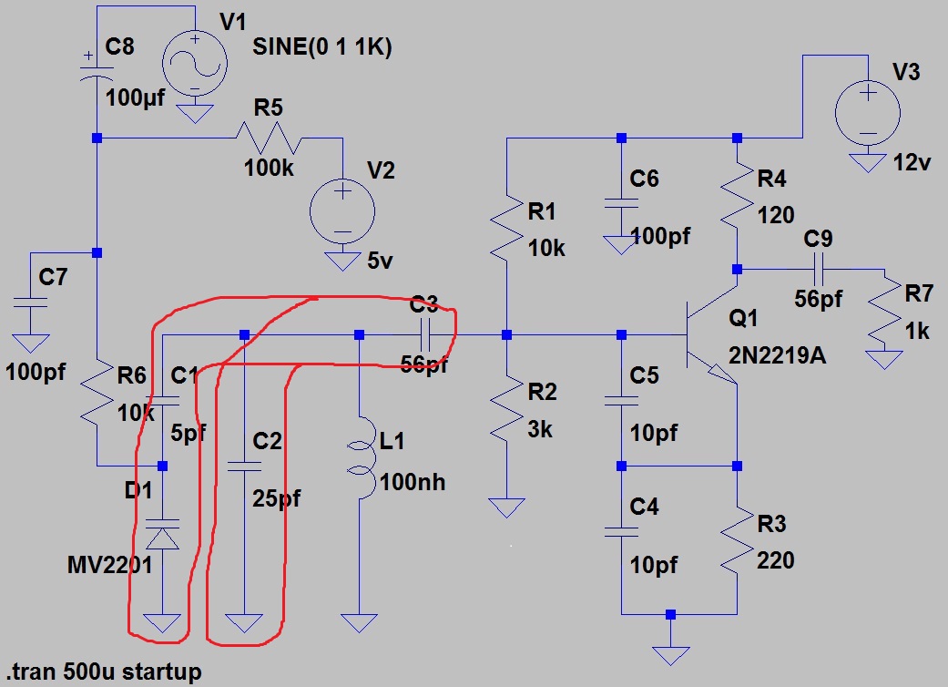
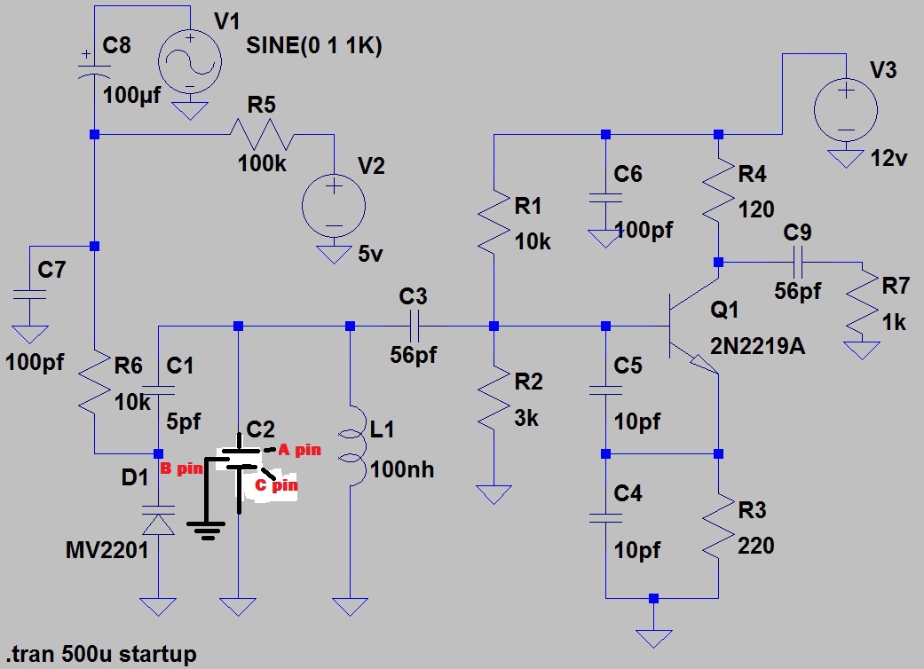
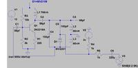
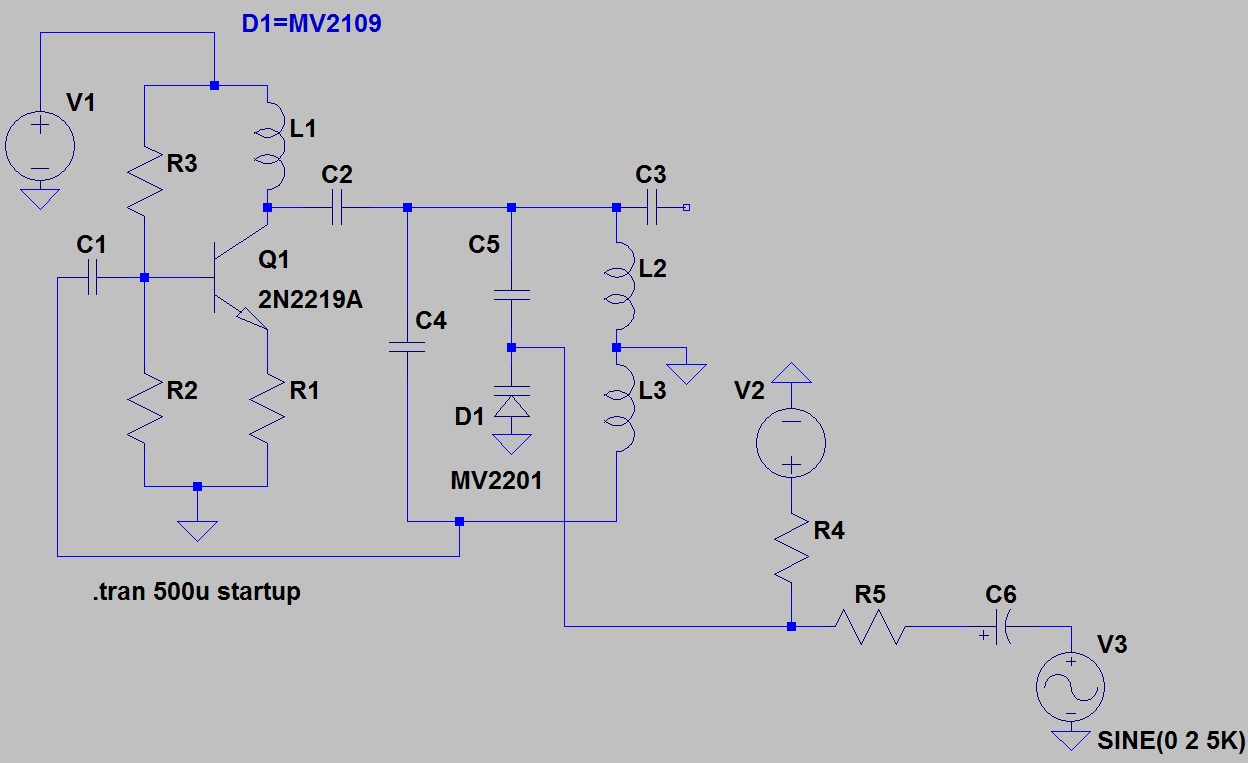
1)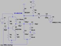
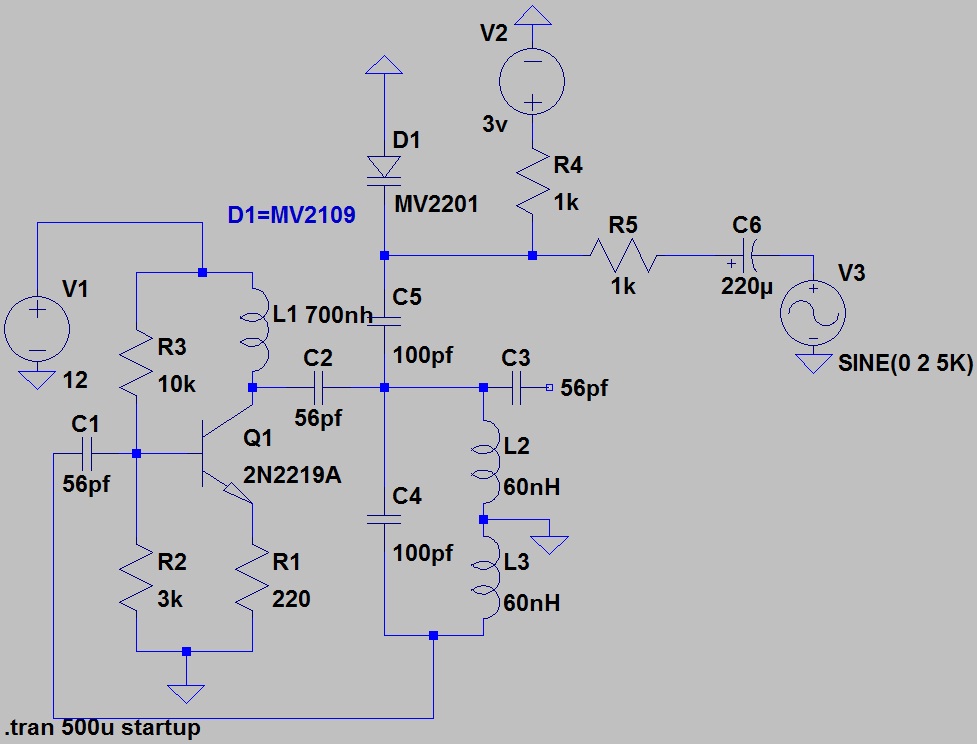
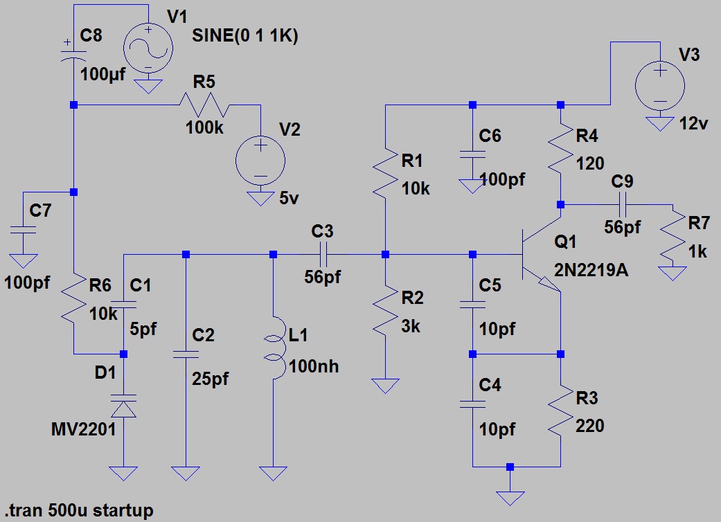
2)
now guys please please tell me which will configuration is correct..
in the first schematic the D1 anode is DIRECTLY grounded,in order to get biased by 3V....
IN 2 schematic,as i think the D1 anode is grounded by the ground connection in between the 2 inductors...
so people .please tell me which configuration is correct..................its my biggest confusion of life......
plz plz help me :-(
here i have made two different circuits.....but i have a big big doubt that which is correct and which is wrong...
1)
2)
now guys please please tell me which will configuration is correct..
in the first schematic the D1 anode is DIRECTLY grounded,in order to get biased by 3V....
IN 2 schematic,as i think the D1 anode is grounded by the ground connection in between the 2 inductors...
so people .please tell me which configuration is correct..................its my biggest confusion of life......
plz plz help me :-(
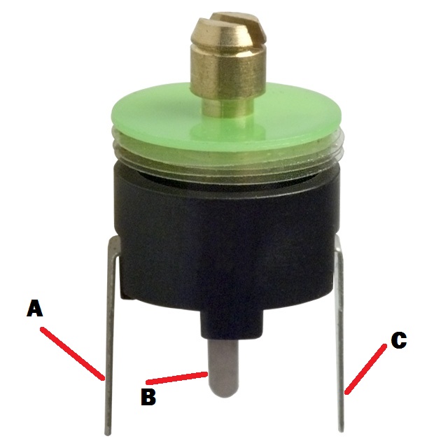
")