Continue to Site

Welcome to EDAboard.com

Welcome to our site! EDAboard.com is an international Electronics Discussion Forum focused on EDA software, circuits, schematics, books, theory, papers, asic, pld, 8051, DSP, Network, RF, Analog Design, PCB, Service Manuals... and a whole lot more! To participate you need to register. Registration is free. Click here to register now.

Overheating LM2596S-5 - Help me fix my first board design

avner_g

Junior Member level 2
Joined
Nov 25, 2023
Messages
22
Helped
0
Reputation
0
Reaction score
0
Trophy points
1
Activity points
227
So I decided I was going to design and build my first PCB and do (yet another) irrigation controller and moisture sensors.
First and foremost, it was great fun. Learning KiCAD, designing everything.

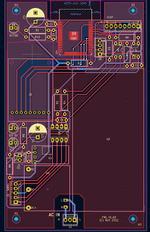
I made the design based on AC24V input (as the pumps require) and, a fairly simple and straightforward diode bridge, and 2 VRegs (to 5V and then 3V3). Here is it: https://github.com/theDontKnowGuy/sprinklers

However, it is not working as expected; the LM2596S-5 (datasheet) got hot in less than a minute to the level I couldn't touch it with my finger. Also a burn smell came out.
I quickly disconnected it and tried another board with AC12V. This time, it got very hot but took longer. Like 2 minutes.

I would appreciate it if you could take a peek at the design https://github.com/theDontKnowGuy/sprinklers to figure out which mistake we made.

I have made several measurements with my digital oscillometer, which I have also attached.
Someone suggested I run the feedback wire close to the inductor, which I did. I removed it and tried with a strad, but it didn't help either.

The main hint I have is that the over heating occurs also when I supply DC, not only AC.

What I am doing wrong???

Slide1.png
Slide2.png
Slide3.png

Slide1.png
Slide2.png
Slide3.png
Slide4.png
Slide12.png
Slide11.png
Slide10.png
Slide9.png
Slide8.png
Slide7.png
 
The PCB is far from optimal but I think the basic problem is simply that you have almost no heatsink. Although the LM2596-5 is rated at 3A, you will see from the data sheet that is at 25C. As the temperature increases, the rating has to be reduced. I would suggest you redesign the PCB so the copper area under the regulator is as large as possible so it can 'spread' the heat better. Use the lower side of the board as much as possible and flood fill it with copper, adding as many via holes as you can reasonably fit underneath the regulator tab so the via and solder conduct the heat away. If you can't solder the tab directly to the PCB, still increase the copper area as much as possible and add a mounting hole so you can screw the regulator down to it with a heat conductive pad underneath.

Remember that although switching regulators are more efficient than linear ones, you are still dropping something around 27 volts across it at the total current drawn by all the circuit.

Also check D5, I can't see what type it is but a fast recovery diode must be used.

Brian.
 
Hey @betwixt and thanks for taking a look.
Thing is, this component is not just getting hot. In under 30 seconds you can boil the ocean with it and it starts smells, even when:
1. using DC ~30V.
2. the load downstream is like 120mA (for the ESP32) and nothing else.

Is it only a hit sync problem? My guts tell me otherwise, but I am a newbie hence I ask.
Thanks again.
 
Some of the components don't have any values, can you tell us exactly what type of diode D5 is and the value of the inductor.
Incidentally, if you have the WiFi enabled in the ESP32 it can take almost 300mA at peaks.

Brian.
 
Sure @betwixt!

D5 : 40V 1A 520mV@1A SMA(DO-214AC) Schottky Barrier Diodes (SBD) ROHS datsheet
L1: 3A 33uH ±20% SMD,12x12mm Power Inductors ROHS datasheet
C5,C6: 470uF 25V ±20% 440mA@100kHz Plugin,D10xL12.5mm Aluminum Electrolytic Capacitors - Leaded ROHS datasheet
C1,C3,C7,C8: 50V 10uF X5R ±10% 0805 Multilayer Ceramic Capacitors MLCC - SMD/SMT ROHS datasheet

BTW, do you think according to the images I attached, that I do have a rining problem on the feedback line?
 
Just an off chance, is scope set for low freq bandwidth on vert channel ?

Its possible part, due to layout, in oscillation and you are not seeing it. Use
FFT function to see if there is a spur of significance. And use 10x on your probe.

If AC in is not isolated observe probing precautions :


To isure you dont hose your scope.


Regards, Dana.
 
Unfortunately the component values given in post #1 and post #5 neither fit the layout nor the schematic. E.g. C8 is according to schematic connected to switching node. Layout shows also C8 in this place, chip size is rather 0402 than 0805. Connecting 10 uF in this place would block switching operation.
--- Updated ---

PCB layout is incredibly bad, firstly GND wiring, secondly other power nets. GND and power nets should be specified with 0.3 mm minimal width and use wider traces and copper pours or meshed topology where possible.
 
Last edited:
The biggest problem is the lack of design specs, especially thermal design specs and layout.

Keep your AC-DC power away from uC inputs if you want to sense anything.

Using 3.3Vref instead of LDO Vref for analog will need additional filtering.

Try to eliminate the need for 5V logic by using 1.5V threshold 3.3V logic with remote terminators to suppress pump EMI, if possible.
Thus use 3.3V converter only.

The ground planes serve to attenuate crosstalk, spurious oscillations and dissipate heat. ~ 5 cm^2/W.
Use twisted pairs to peripherals or STP wire.
Add test points and use suitable connectors.
Include AC cap on DC out to measure ripple with 50 Ohm load as a test point.

Your layout should then look like this. Then you can make use of inexpensive ESP32 boards.

Note that even with this amount of double-sided ground plane, you still get a "hot surface". 3.3V @ 1A from 12 to 24V input.

1700942318229.png


Perhaps consider a kit design with LCD see how these are designed.
 
Last edited:
OK. thank you very much @D.A.(Tony)Stewart, @FvM , @danadakk , and @betwixt for your insightful comments (even if sometimes rough:) comments.
Remember that I am a senior software engineer and manager, but a total newbie in the circuit design field.
So I took some of the advice (mostly the ones I could understand) and made changes to the schematic design to begin with.
I would appreciate comments on the schematic design (before I make the physical design).
As a reminder, I still got noise after the LM2695 and the second to the chip.

TL;DR: I am building a (yet another) irrigation controller and moisture sensors (which is the exact same circuit just without the relays).

My question: Have I chosen the correct components and structure to smooth the AC 24V I am getting in?

Thanks in advance.
Screenshot 2023-11-29 at 14.20.46.png


D9 to D14 should be across the relay coil, not in series with it. Wire it cathode to supply so it doesn't normally conduct. The back EMF as the relay turns off has the opposite polarity to the voltage applied to operate it so the diode WILL conduct and clamp the voltage to a safe level.

The may be a problem in the design which isn't immediately obvious. Check the requirements of the ESP32 to boot into running mode. By leaving IO0 floating, it might try to start up in bootloader mode. You should probably add a pull-up resistor (~10K) between IO0 and VDD.

For the layout, try to keep the ground area as large as possible and use thicker tracks for the supply lines. Kicad has a great flood fill facility, draw a boundary around the whole board, top and bottom sides, select ground as the connection node and flood fill them. If you are using the WiFi or Bluetooth in the ESP32, add a "keep out" area before flood filling or it will shield the antenna. Also try to keep tracks away from the antenna area of the module.

Brian.
 
Hi,

My comment to the schematic:
Wrong:
* the wiring of the diodes at the relay coils. Please do a search on "free wheeling diodes on relays"

Technically not wrong, but makes it difficult to read the schematic: (Please review how other schematics are drawn)
* use GND symbols
* don´t use different names on the same signal: GRD vs GND1
* use power supply symbols
* don´t run the signals through the body of the devices
* signal flow is: from left to right
* use separate sheets: for power supply and the rest
* don´t write lengthy text into a schematic. Better use [D21] with the value of [1N4148] for example. (1N4148 tells much more than all your text)
(Better use a BOM / text / Excel with these informations)

Hints:
* you may use 1x TPL7407 (or similar) instead of: 6 x R, 6x MOSFET, 6x diode
* fuses at the relay outputs?
* snubbers or varistors across the relay contacts?
* sure you want to use TXD and TXD externally, they are already used internally.
* mind not to leave any (unused) input floating
* consider to use a capacitor at analog inputs
* ESD protection?


Klaus
 
The capacitors on the power supply bus are good for noise suppression, but you also may wish to consider series ferrites depending on your ripple/noise spec. They do wonders at cleaning up higher-frequency noise, for a relatively low cost.
 
OK!! Thank you @PlanarMetamaterials, @KlausST, @betwixt and @D.A.(Tony)Stewart, for your educated suggestions.
I have implemented some of them, the ones I could figure out, and I think this got improved by a number of factors.
Here is another brave attempt.
Comments will be welcomed if this is going to do the job.
I specifically question two things:
1. the FerriteBead, which I'm still not sure where to place and what spec is required
2. Are the capacitors, and the added varistor the right spec and will do the filtering? Too many of them?

Remember, you are talking to a hobbyist that it is his first PCB project :)

Thanks much!
Screenshot 2023-12-03 at 10.37.46.png
 
Much better.
I think there may still be a connection error though, check the circuitry around the sensor. All RV1 does is change the current through the sensor, there is no connection to the ESP32 to actually measure it.
In your software make sure you enable the pull-up or pull down sources on all the unused pins, this will prevent them 'floating' and potentially triggering unwanted actions in the MCU. It will also help to reduce susceptibility to noise.
On the PCB layout, you will still need to provide a copper area to conduct heat away from the regulator, either by screwing its tab to the board, via an insulating pad or with a metal finned heatsink. Make the tracks carrying 5V and 3.3V as wide as possible, at least 0.5mm and preferably more. Finally, draw a boundary around the board edge and use Kicads copper pour to flood fill and join all the grounds together on both board surfaces.

I have attached an example of the thicker power tracks and flood fill from a recent project (which hasn't had any issues in a years continuous operation). The resolution is deliberately reduced, the ESP32 pins are not really joined together!

Brian.
 

Attachments

  • Screenshot_20231203_093233.png
    Screenshot_20231203_093233.png
    67.3 KB · Views: 56
If I understand right, new post #13 schematic is a draft, not yet implemented as PCB. Some additional comments
- C7 has no sufficient voltage rating for 24 VAC circuit input, and nearly no capacitance at 35 to 40 V DC.
- I read AMS1117 datasheet so that it's no necessarily stable with ceramic output capacitors. Unfortunately they don't specify minimal ESR of output capacitors, but suggest tantal output capacitor which has considerably higher ESR than 10 uF MLCC. Other 1117 datasheets, e.g. original LM1117 have more information about output capacitor problem
- I'm missing bypass capacitors for ESP32 power supply pins. I agree with betwixt, RF transmitter PCB should have overall ground plane, except for the antenna area.
 
thanks @FvM! Yes, I will redo my PCB design once I figure out this one.
C7 - understood.
C8 - Hope I got you right. I replaced it with https://datasheet.lcsc.com/lcsc/2304140030_KEMET-T491D106K035AT_C122299.pdf
1. Is it any good?
2. Mostly, I am confused with the FerriteBead, which I'm still not sure where to place and what spec is required.
3. Is the varistor placed correctly and has the right spec?

I also fixed @betwixt catch on the sensor and will follow instructions on the PCB later.

1701601860062.png
 
Don't lose sleep over the ferrite bead. They can be useful in some situations but I don't think this is one of them. They can 'trap' current spikes but if you are sensible with board layout they shouldn't be a problem anyway. If you really want to add them, put one on each of the incoming AC wires, it may help to stop high frequency interference in and out.

I note your relays are wired differently, I'm not sure if that is intentional. K1 is a 'master' AC switch for all the others. Also be careful with the GNDA connection on J1 thru J6. It isn't wrong but be sure current through that line cannot disturb current in GND, particularly if external devices on J1 - J6 also have their own ground connections.

Brian.
 
Hi,

again I want to remind you to use a capacitor at the ADC input ... especially when the sensor is installed remote and picks up noise on the cable.

Klaus
 
@KlausST I need some help here. I understand you suggest I place a cap on the AC input before the rectifier bridge.
Can you hint me please which kind of capacitor I am looking for?
On non-polarized capacitors, I saw only ones with a nF capacitance.

Thanks!
 
Klaus means on the ADC input, not the AC input. ADC input is the pin the sensor voltage is connected to. I would suggest 100nF between whichever pin it is and ground, as close to the ESP32 as possible. From your schematic it looks like IO32 is used as the sensor input but we don't know what sensor it is and hence what output it will produce.

Brian.
 

LaTeX Commands Quick-Menu:

Similar threads

Part and Inventory Search

Welcome to EDABoard.com

Sponsor

Back
Top